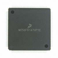
MC56F8147VPYE Freescale Semiconductor, MC56F8147VPYE Datasheet - Page 36

MC56F8147VPYE
Manufacturer Part Number
MC56F8147VPYE
Description
IC DSP 16BIT 40MHZ 160-LQFP
Manufacturer
Freescale Semiconductor
Series
56F8xxxr
Datasheet
1.MC56F8147VPYE.pdf
(172 pages)
Specifications of MC56F8147VPYE
Core Processor
56800
Core Size
16-Bit
Speed
40MHz
Connectivity
EBI/EMI, SCI, SPI
Peripherals
POR, PWM, WDT
Number Of I /o
76
Program Memory Size
128KB (64K x 16)
Program Memory Type
FLASH
Ram Size
4K x 16
Voltage - Supply (vcc/vdd)
2.25 V ~ 3.6 V
Data Converters
A/D 16x12b
Oscillator Type
External
Operating Temperature
-40°C ~ 105°C
Package / Case
160-LQFP
Data Bus Width
16 bit
Processor Series
MC56F81xx
Core
56800E
Data Ram Size
4 KB
Interface Type
SPI, SCI, CAN
Maximum Clock Frequency
40 MHz
Number Of Programmable I/os
76
Number Of Timers
2
Maximum Operating Temperature
+ 105 C
Mounting Style
SMD/SMT
Minimum Operating Temperature
- 40 C
On-chip Adc
4 x 12 bit, 4 Channel
Lead Free Status / RoHS Status
Lead free / RoHS Compliant
Eeprom Size
-
Lead Free Status / Rohs Status
Lead free / RoHS Compliant
Available stocks
Company
Part Number
Manufacturer
Quantity
Price
Company:
Part Number:
MC56F8147VPYE
Manufacturer:
FREESCAL
Quantity:
253
Company:
Part Number:
MC56F8147VPYE
Manufacturer:
Freescale Semiconductor
Quantity:
10 000
36
Table 2-2 Signal and Package Information for the 160-Pin LQFP and MBGA (Continued)
Signal Name
(GPIOE10)
(GPIOE11)
(GPIOE12)
(GPIOE13)
RESET
RSTO
IRQA
IRQB
TD0
TD1
TD2
TD3
129
130
131
132
Pin
No.
65
66
98
97
Ball
D10
B10
A10
E10
No.
J14
J13
K9
P9
Schmitt
Schmitt
Schmitt
Schmitt
Output
Output
Output
Input/
Input/
Type
Input
Input
56F8347 Technical Data, Rev.11
enabled
enabled
enabled
During
pull-up
pull-up
pull-up
Output
Reset
Input,
Input,
Input,
State
TD0 - 3 — Timer D, Channels 0, 1, 2 and 3
Port E GPIO — These GPIO pins can be individually
programmed as input or output pins.
At reset, these pins default to Timer functionality.
To deactivate the internal pull-up resistor, clear the
appropriate bit of the GPIOE_PUR register. See
for details.
External Interrupt Request A and B — The IRQA and
IRQB inputs are asynchronous external interrupt requests
during Stop and Wait mode operation. During other
operating modes, they are synchronized external interrupt
requests, which indicate an external device is requesting
service. They can be programmed to be level-sensitive or
negative-edge triggered.
To deactivate the internal pull-up resistor, set the IRQ bit in
the SIM_PUDR register. See
Reset — This input is a direct hardware reset on the
processor. When RESET is asserted low, the device is
initialized and placed in the reset state. A Schmitt trigger
input is used for noise immunity. When the RESET pin is
deasserted, the initial chip operating mode is latched from
the EXTBOOT pin. The internal reset signal will be
deasserted synchronous with the internal clocks after a fixed
number of internal clocks.
To ensure complete hardware reset, RESET and TRST
should be asserted together. The only exception occurs in a
debugging environment when a hardware device reset is
required and the JTAG/EOnCE module must not be reset. In
this case, assert RESET but do not assert TRST.
Note: The internal Power-On Reset will assert on initial
power-up.
To deactivate the internal pull-up resistor, set the RESET bit
in the SIM_PUDR register. See
Reset Output — This output reflects the internal reset state
of the chip.
Signal Description
Part 6.5.6
Part 6.5.6
Freescale Semiconductor
for details.
for details.
Part 6.5.6
Preliminary


