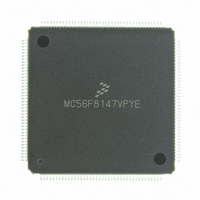
MC56F8147VPYE Freescale Semiconductor, MC56F8147VPYE Datasheet - Page 45

MC56F8147VPYE
Manufacturer Part Number
MC56F8147VPYE
Description
IC DSP 16BIT 40MHZ 160-LQFP
Manufacturer
Freescale Semiconductor
Series
56F8xxxr
Datasheet
1.MC56F8147VPYE.pdf
(172 pages)
Specifications of MC56F8147VPYE
Core Processor
56800
Core Size
16-Bit
Speed
40MHz
Connectivity
EBI/EMI, SCI, SPI
Peripherals
POR, PWM, WDT
Number Of I /o
76
Program Memory Size
128KB (64K x 16)
Program Memory Type
FLASH
Ram Size
4K x 16
Voltage - Supply (vcc/vdd)
2.25 V ~ 3.6 V
Data Converters
A/D 16x12b
Oscillator Type
External
Operating Temperature
-40°C ~ 105°C
Package / Case
160-LQFP
Data Bus Width
16 bit
Processor Series
MC56F81xx
Core
56800E
Data Ram Size
4 KB
Interface Type
SPI, SCI, CAN
Maximum Clock Frequency
40 MHz
Number Of Programmable I/os
76
Number Of Timers
2
Maximum Operating Temperature
+ 105 C
Mounting Style
SMD/SMT
Minimum Operating Temperature
- 40 C
On-chip Adc
4 x 12 bit, 4 Channel
Lead Free Status / RoHS Status
Lead free / RoHS Compliant
Eeprom Size
-
Lead Free Status / Rohs Status
Lead free / RoHS Compliant
Available stocks
Company
Part Number
Manufacturer
Quantity
Price
Company:
Part Number:
MC56F8147VPYE
Manufacturer:
FREESCAL
Quantity:
253
Company:
Part Number:
MC56F8147VPYE
Manufacturer:
Freescale Semiconductor
Quantity:
10 000
4.4 Data Map
Note: Data Flash is NOT available on the 56F8147 device.
Freescale Semiconductor
Preliminary
1. Two words are allocated for each entry in the vector table. This does not allow the full address range to be referenced from the
2. If the VBA is set to 0200 (or VBA = 0000 for Mode 1, EMI_MODE = 0), the first two locations of the vector table are the chip
SCI0
SCI0
SCI0
SCI0
ADCB
ADCA
ADCB
ADCA
PWMB
PWMA
PWMB
PWMA
core
1. All addresses are 16-bit Word addresses, not byte addresses.
2. In the Operating Mode Register (OMR).
3. The Data RAM is organized as a 2K x 32-bit memory to allow single-cycle long-word operations.
X:$FF FFFF
X:$FF 0000
X:$FF FEFF
X:$01 0000
X:$00 FFFF
X:$00 F000
X:$00 EFFF
X:$00 2000
X:$00 1FFF
X:$00 1000
X:$00 0FFF
X:$00 0000
Peripheral
vector table, providing only 19 bits of address.
reset addresses; therefore, these locations are not interrupt vectors.
Begin/End
Address
Number
Vector
68
69
71
72
73
74
75
76
77
78
79
80
81
Table 4-5 Interrupt Vector Table Contents
EOnCE
256 locations allocated
External Memory
On-Chip Peripherals
4096 locations allocated
External Memory
On-Chip Data Flash
8KB
On-Chip Data RAM
8KB
3
Priority
Level
0-2
0-2
0-2
0-2
0-2
0-2
0-2
0-2
0-2
0-2
0-2
0-2
- 1
Table 4-6 Data Memory Map
EX = 0
Vector Base
Address +
56F8347 Technical Data, Rev.11
P:$9C
P:$88
P:$8A
P:$8E
P:$90
P:$92
P:$94
P:$96
P:$98
P:$9A
P:$9E
P:$A0
P:$A2
2
SCI 0 Transmitter Empty
SCI 0 Transmitter Idle
Reserved
SCI 0 Receiver Error
SCI 0 Receiver Full
ADC B Conversion Compete / End of Scan
ADC A Conversion Complete / End of Scan
ADC B Zero Crossing or Limit Error
ADC A Zero Crossing or Limit Error
Reload PWM B
Reload PWM A
PWM B Fault
PWM A Fault
SW Interrupt LP
EOnCE
256 locations allocated
External Memory
On-Chip Peripherals
4096 locations allocated
External Memory
1
Interrupt Function
1
(Continued)
EX = 1
Data Map
45


