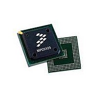
MPC5125YVN400 Freescale Semiconductor, MPC5125YVN400 Datasheet - Page 52

MPC5125YVN400
Manufacturer Part Number
MPC5125YVN400
Description
IC MCU 32BIT E300 324TEPBGA
Manufacturer
Freescale Semiconductor
Series
MPC51xxr
Datasheets
1.MPC5125YVN400.pdf
(92 pages)
2.MPC5125YVN400.pdf
(8 pages)
3.MPC5125YVN400.pdf
(2 pages)
4.MPC5125YVN400.pdf
(1064 pages)
Specifications of MPC5125YVN400
Core Processor
e300
Core Size
32-Bit
Speed
400MHz
Connectivity
CAN, EBI/EMI, Ethernet, I²C, USB OTG
Peripherals
DMA, WDT
Number Of I /o
64
Program Memory Type
ROMless
Ram Size
32K x 8
Voltage - Supply (vcc/vdd)
1.33 V ~ 1.47 V
Oscillator Type
External
Operating Temperature
-40°C ~ 125°C
Package / Case
324-PBGA
Processor Series
MPC51xx
Core
e300
Data Bus Width
32 bit
Development Tools By Supplier
TWR-MPC5125-KIT, TWR-SER, TWR-ELEV, TOWER
Maximum Clock Frequency
400 MHz
Operating Supply Voltage
1.4 V
Maximum Operating Temperature
+ 125 C
Mounting Style
SMD/SMT
Data Ram Size
32 KB
I/o Voltage
3.3 V
Interface Type
CAN, I2C
Minimum Operating Temperature
- 40 C
Program Memory Size
32 bit
Cpu Speed
400MHz
Embedded Interface Type
CAN, I2C, SPI, UART, USB
Digital Ic Case Style
TEPBGA
No. Of Pins
324
Rohs Compliant
Yes
Cpu Family
MPC5xx
Device Core Size
32b
Frequency (max)
400MHz
Total Internal Ram Size
32KB
Instruction Set Architecture
RISC
Operating Temp Range
-40C to 85C
Operating Temperature Classification
Industrial
Mounting
Surface Mount
Pin Count
324
Lead Free Status / RoHS Status
Lead free / RoHS Compliant
Eeprom Size
-
Program Memory Size
-
Data Converters
-
Lead Free Status / Rohs Status
Lead free / RoHS Compliant
Available stocks
Company
Part Number
Manufacturer
Quantity
Price
Company:
Part Number:
MPC5125YVN400
Manufacturer:
Freescale Semiconductor
Quantity:
135
Company:
Part Number:
MPC5125YVN400
Manufacturer:
LTC
Quantity:
29
Company:
Part Number:
MPC5125YVN400
Manufacturer:
Freescale Semiconductor
Quantity:
10 000
Electrical and Thermal Characteristics
NOTES:
1
2
3
4
5
4.3.5.3
52
Address and control output hold time
relative to MCK rising edge
DQ and DM output setup time relative to
DQS
DQ and DM output hold time relative to
DQS
DQS-DQ skew for DQS and associated
DQ inputs
DQS window position related to CAS
read command
Clock cycle time, CL = x
MCK AC differential crosspoint voltage
CK HIGH pulse width
CK LOW pulse width
Skew between MCK and DQS transitions
Address and control output setup time
relative to MCK rising edge
Address and control output hold time
relative to MCK rising edge
DQ and DM output setup time relative to
DQS
DQ and DM output hold time relative to
DQS
DQS-DQ skew for DQS and associated
DQ inputs
DQS window position related to CAS
read command
Measured with clock pin loaded with differential 100 Ω termination resistor.
Measured with all outputs except the clock loaded with 50 Ω termination resistor to V
All transitions measured at mid-supply (V
In this window, the first rising edge of DQS should occur. From the start of the window to DQS rising edge, DQS should be low.
The window position is given for t
MobileDDR/LPDDR SDRAM device. For other values of t
Parameter
Parameter
DDR2 SDRAM AC Timing Specifications
Table 22. MobileDDR/LPDDR SDRAM Timing Specifications (continued)
Table 23. DDR2 (DDR2-400) SDRAM Timing Specifications
At recommended operating conditions with V
At recommended operating conditions with V
DQSEN
MPC5125 Microcontroller Data Sheet, Rev. 3
t
t
t
t
t
Symbol
DH1(base)
DS1(base)
= 2.0 t
t
t
Symbol
DS1(base)
DH1(base)
OH(base)
t
OS(base)
OH(base)
V
t
t
DQSEN
DD_IO_MEM
t
t
DQSEN
DQSQ
DQSQ
DQSS
OX-AC
t
t
t
CK
CH
CL
CK
(RDLY = 2, HALF DQS DLY = QUART DQS DLY = 0) with CL = 3
(V
/2).
DD_IO_MEM
– (t
– (t
t
CK
t
t
DQSEN
2t
t
t
t
t
CK
CK
CK
CK
CK
CK
CK
CK
CK
/2 – 1000
2.5t
/4 – 750
/4 – 750
−0.25
5000
/2 − 750
/2 − 750
/4 − 500
/4 − 500
Min
0.47
0.47
Min
/4 – 600)
/4 – 600)
– 500
CK
, the window position is shifted accordingly.
× 0.5) – 0.1 (V
DD_IO_MEM
DD_IO_MEM
DD_IO_MEM
3t
3t
t
t
CK
CK
DD_IO_MEM
CK
CK
/4 – 600
Max
/4 − 600
Max
0.53
0.53
0.25
of ±5%
of ±5%
—
—
—
– 1000
—
—
—
—
—
+ 1500
× 0.5) + 0.1
/2.
Freescale Semiconductor
Unit Notes SpecID
Unit Notes SpecID
t
t
t
ps
ps
ps
ps
ps
ps
ps
ps
ps
ps
ps
ps
CK
CK
CK
V
1,2,3,4,5
1,2,3,4,
2,3
2,3
2,3
2,3
1,3
1,3
2,3
2,3
2,3
2,3
3
1
3
5
A5.10
A5.11
A5.10
A5.11
A5.7
A5.8
A5.9
A5.1
A5.2
A5.3
A5.4
A5.5
A5.6
A5.7
A5.8
A5.9


