M30845FJGP#U3 Renesas Electronics America, M30845FJGP#U3 Datasheet - Page 234
M30845FJGP#U3
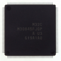
Manufacturer Part Number
M30845FJGP#U3
Description
IC M32C MCU FLASH 512K 144LQFP
Manufacturer
Renesas Electronics America
Series
M16C™ M32C/80r
Specifications of M30845FJGP#U3
Core Processor
M32C/80
Core Size
16/32-Bit
Speed
32MHz
Connectivity
CAN, I²C, IEBus, SIO, UART/USART
Peripherals
DMA, PWM, WDT
Number Of I /o
121
Program Memory Size
512KB (512K x 8)
Program Memory Type
FLASH
Ram Size
24K x 8
Voltage - Supply (vcc/vdd)
3 V ~ 5.5 V
Data Converters
A/D 34x10b, D/A 2x8b
Oscillator Type
Internal
Operating Temperature
-40°C ~ 85°C
Package / Case
144-LQFP
Lead Free Status / RoHS Status
Lead free / RoHS Compliant
Eeprom Size
-
Available stocks
Company
Part Number
Manufacturer
Quantity
Price


R
R
M
e
E
3
. v
J
2
Table 17.8 Pin Settings in UART Mode (1)
Table 17.9 Pin Settings (2)
Table 17.10 Pin Settings (3)
0
NOTES:
NOTES:
C
P6
P6
P6
P6
P6
P6
P6
P6
P7
P7
P7
P7
P9
P9
P9
P9
P9
P9
P9
P9
1
9
0 .
8 /
B
1. P7
1. Set the PD9 and PS3 registers set immediately after the PRC2 bit in the PRCR register is set to "1" (write enable).
Port
Port
Port
0
1
2
3
4
5
6
7
0 (1)
1 (1)
2
3
0
1
2
3
4
5
6
7
0
1
4
Do not generate an interrupt or a DMA transfer between the instruction to set to the PRC2 bit to "1" and the
instruction to set the PD9 and PS3 registers.
0
3
G
J
6
0
u
o r
0 -
. l
and P7
u
0
1
, 7
0
p
__________
__________
__________
__________
__________
__________
__________
__________
__________
__________
1
CTS0 input
RTS0 output
CLK0 input
RxD0 input
TxD0 output
CTS1 input
RTS1 output
CLK1 input
RxD1 input
TxD1 output
TxD2 output
RxD2 input
CLK2 input
CTS2 input
RTS2 output
CLK3 input
RxD3 input
TxD3 output
CTS3 input
RTS3 output
CTS4 input
RTS4 output
CLK4 input
TxD4 output
RxD4 input
(
2
M
0
1
0
3
Function
Function
Function
are ports for the N-channel open drain output.
5
2
C
8 /
Page 211
, 4
M
3
2
C
f o
8 /
PS0 Register
PS0_0=0
PS0_0=1
PS0_1=0
PS0_2=0
PS0_3=1
PS0_4=0
PS0_4=1
PS0_5=0
PS0_6=0
PS0_7=1
PS1 Register
PS1_0=1
PS1_1=0
PS1_2=0
PS1_3=0
PS1_3=1
PS3 Register
PS3_0=0
PS3_1=0
PS3_2=1
PS3_3=0
PS3_3=1
PS3_4=0
PS3_4=1
PS3_5=0
PS3_6=1
PS3_7=0
4
4
) T
9
5
(1)
PSL0 Register
PSL0_4=0
–
–
–
PSL3 Register
–
–
PSL3_2=0
PSL3_3=0
–
PSL3_4=0
–
PSL3_5=0
–
–
–
–
–
–
–
–
PSL1 Register
PSL1_0=0
–
–
–
PSL1_3=0
Setting
Setting
Setting
PD6 Register
PD6_0=0
–
PD6_1=0
PD6_2=0
–
PD6_4=0
–
PD6_5=0
PD6_6=0
–
PSC Register
PSC_0=0
–
–
–
PSC_3=0
PD9 Register
PD9_0=0
PD9_1=0
–
PD9_3=0
–
PD9_4=0
–
PD9_5=0
–
PD9_7=0
(1)
17. Serial I/O (UART)
PD7 Register
–
PD7_1=0
PD7_2=0
PD7_3=0
–
Related parts for M30845FJGP#U3
Image
Part Number
Description
Manufacturer
Datasheet
Request
R

Part Number:
Description:
KIT STARTER FOR M16C/29
Manufacturer:
Renesas Electronics America
Datasheet:

Part Number:
Description:
KIT STARTER FOR R8C/2D
Manufacturer:
Renesas Electronics America
Datasheet:

Part Number:
Description:
R0K33062P STARTER KIT
Manufacturer:
Renesas Electronics America
Datasheet:

Part Number:
Description:
KIT STARTER FOR R8C/23 E8A
Manufacturer:
Renesas Electronics America
Datasheet:

Part Number:
Description:
KIT STARTER FOR R8C/25
Manufacturer:
Renesas Electronics America
Datasheet:

Part Number:
Description:
KIT STARTER H8S2456 SHARPE DSPLY
Manufacturer:
Renesas Electronics America
Datasheet:

Part Number:
Description:
KIT STARTER FOR R8C38C
Manufacturer:
Renesas Electronics America
Datasheet:

Part Number:
Description:
KIT STARTER FOR R8C35C
Manufacturer:
Renesas Electronics America
Datasheet:

Part Number:
Description:
KIT STARTER FOR R8CL3AC+LCD APPS
Manufacturer:
Renesas Electronics America
Datasheet:
Part Number:
Description:
KIT STARTER FOR RX610
Manufacturer:
Renesas Electronics America
Datasheet:

Part Number:
Description:
KIT STARTER FOR R32C/118
Manufacturer:
Renesas Electronics America
Datasheet:

Part Number:
Description:
KIT DEV RSK-R8C/26-29
Manufacturer:
Renesas Electronics America
Datasheet:

Part Number:
Description:
KIT STARTER FOR SH7124
Manufacturer:
Renesas Electronics America
Datasheet:

Part Number:
Description:
KIT STARTER FOR H8SX/1622
Manufacturer:
Renesas Electronics America
Datasheet:

Part Number:
Description:
KIT DEV FOR SH7203
Manufacturer:
Renesas Electronics America
Datasheet: