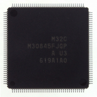
M30845FJGP#U3 Renesas Electronics America, M30845FJGP#U3 Datasheet - Page 496

M30845FJGP#U3
Manufacturer Part Number
M30845FJGP#U3
Description
IC M32C MCU FLASH 512K 144LQFP
Manufacturer
Renesas Electronics America
Series
M16C™ M32C/80r
Specifications of M30845FJGP#U3
Core Processor
M32C/80
Core Size
16/32-Bit
Speed
32MHz
Connectivity
CAN, I²C, IEBus, SIO, UART/USART
Peripherals
DMA, PWM, WDT
Number Of I /o
121
Program Memory Size
512KB (512K x 8)
Program Memory Type
FLASH
Ram Size
24K x 8
Voltage - Supply (vcc/vdd)
3 V ~ 5.5 V
Data Converters
A/D 34x10b, D/A 2x8b
Oscillator Type
Internal
Operating Temperature
-40°C ~ 85°C
Package / Case
144-LQFP
Lead Free Status / RoHS Status
Lead free / RoHS Compliant
Eeprom Size
-
Available stocks
Company
Part Number
Manufacturer
Quantity
Price
- Current page: 496 of 531
- Download datasheet (4Mb)
M
R
R
e
E
3
. v
J
2
Table 27.3 Power Supply Ripple
Figure 27.2 Power Supply Fluctuation Timing
0
f
V
V
C
27.5.3 PLL Frequency Synthesizer
r (
27.5.4 External Clock
27.5.5 Clock Divide Ratio
27.5.6 Power Consumption Control
1
9
P
C
f
Power Supply Ripple Tolerable Frequency
(V
p i
V
Power Supply Ripple Amplitude
Voltage
8 /
0 .
(ripple)
B
P -
C
S
Stabilize supply voltage to meet the power supply standard when using the PLL frequency synthesizer.
l p
Do not stop an external clock running if the main clock is selected as the CPU clock while the external
clock is applied to the X
Do not set the CM05 bit in the CM0 register to "1" (main clock stopped) while the external clock input is
used for the CPU clock.
Set the PM12 bit in the PM1 register to "0" (no wait state) when changing the MCD4 to MCD0 bit settings
in the MCD register.
Stabilize the main clock, sub clock or PLL clock to switch the CPU clock source to each clock.
p-p(ripple)
| (
CC1
r (
0
y
) e
1
4
27.5.6.1 Wait Mode
p i
0
m
/ V
l p
G
When entering wait mode while the CM02 bit in the CM0 register is set to "1" (peripheral function stop
in wait mode), set the MCD4 to MCD0 bits in the MCD register to maintain 10-MHz CPU clock fre-
quency or less.
When entering wait mode, the instruction queue reads ahead to instructions following the WAIT in-
struction, and the program stops. Write at least 4 NOP instructions after the WAIT instruction.
3
J
b
)
) e
6
u
l o
o r
T
0 -
. l
) |
u
0
1
p
, 7
0
P
P
P
1
(
o
o
o
2
M
w
w
w
0
3
0
r e
r e
r e
2
5
C
S
S
S
u
u
u
8 /
Page 473
p
p
p
, 4
p
p
p
y l
y l
y l
M
R
R
R
3
p i
p i
p i
IN
2
p
p
p
C
e l
e l
e l
pin.
8 /
f o
T
V
V
o
4
l o
l o
4
e l
) T
a t
a t
9
a r
5
g
g
b
e
e
e l
F
F
u l
u l
F
e r
c
c
V
u t
u t
P
CC1
q
t a
t a
u
a
e
a r
o i
o i
n
m
n
n
y c
t e
R
R
V (
a
a
r e
n
e t
C
g
C
e
1
)
V
V
V
V
V
V
f
(ripple)
C
C
C
C
C
C
C
C
C
C
C
C
1
1
1
1
1
1
=
=
=
=
=
=
27. Precautions (Clock Generation Circuit)
5
3
5
3
5
3
V
3 .
V
3 .
V
3 .
V
V
V
M
i
. n
S
a t
T
n
y
d
. p
a
d r
V
M
1
p-p(ripple)
0
0
0
1
0
a
5 .
2 .
1
1 .
0
. x
0
/ V
/ V
U
k
H
H
V
V
m
m
n
z
t i
z
s
s
Related parts for M30845FJGP#U3
Image
Part Number
Description
Manufacturer
Datasheet
Request
R

Part Number:
Description:
KIT STARTER FOR M16C/29
Manufacturer:
Renesas Electronics America
Datasheet:

Part Number:
Description:
KIT STARTER FOR R8C/2D
Manufacturer:
Renesas Electronics America
Datasheet:

Part Number:
Description:
R0K33062P STARTER KIT
Manufacturer:
Renesas Electronics America
Datasheet:

Part Number:
Description:
KIT STARTER FOR R8C/23 E8A
Manufacturer:
Renesas Electronics America
Datasheet:

Part Number:
Description:
KIT STARTER FOR R8C/25
Manufacturer:
Renesas Electronics America
Datasheet:

Part Number:
Description:
KIT STARTER H8S2456 SHARPE DSPLY
Manufacturer:
Renesas Electronics America
Datasheet:

Part Number:
Description:
KIT STARTER FOR R8C38C
Manufacturer:
Renesas Electronics America
Datasheet:

Part Number:
Description:
KIT STARTER FOR R8C35C
Manufacturer:
Renesas Electronics America
Datasheet:

Part Number:
Description:
KIT STARTER FOR R8CL3AC+LCD APPS
Manufacturer:
Renesas Electronics America
Datasheet:

Part Number:
Description:
KIT STARTER FOR RX610
Manufacturer:
Renesas Electronics America
Datasheet:

Part Number:
Description:
KIT STARTER FOR R32C/118
Manufacturer:
Renesas Electronics America
Datasheet:

Part Number:
Description:
KIT DEV RSK-R8C/26-29
Manufacturer:
Renesas Electronics America
Datasheet:

Part Number:
Description:
KIT STARTER FOR SH7124
Manufacturer:
Renesas Electronics America
Datasheet:

Part Number:
Description:
KIT STARTER FOR H8SX/1622
Manufacturer:
Renesas Electronics America
Datasheet:

Part Number:
Description:
KIT DEV FOR SH7203
Manufacturer:
Renesas Electronics America
Datasheet:


