M30845FJGP#U3 Renesas Electronics America, M30845FJGP#U3 Datasheet - Page 335
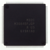
M30845FJGP#U3
Manufacturer Part Number
M30845FJGP#U3
Description
IC M32C MCU FLASH 512K 144LQFP
Manufacturer
Renesas Electronics America
Series
M16C™ M32C/80r
Specifications of M30845FJGP#U3
Core Processor
M32C/80
Core Size
16/32-Bit
Speed
32MHz
Connectivity
CAN, I²C, IEBus, SIO, UART/USART
Peripherals
DMA, PWM, WDT
Number Of I /o
121
Program Memory Size
512KB (512K x 8)
Program Memory Type
FLASH
Ram Size
24K x 8
Voltage - Supply (vcc/vdd)
3 V ~ 5.5 V
Data Converters
A/D 34x10b, D/A 2x8b
Oscillator Type
Internal
Operating Temperature
-40°C ~ 85°C
Package / Case
144-LQFP
Lead Free Status / RoHS Status
Lead free / RoHS Compliant
Eeprom Size
-
Available stocks
Company
Part Number
Manufacturer
Quantity
Price


R
R
M
e
E
3
. v
J
2
NOTES:
NOTES:
Table 22.16 Pin Settings in Clock Synchronous Serial I/O Mode (Communication Units 0 and 1)(1)
Table 22.17 Pin Settings (2)
Table 22.18 Pin Settings (3)
Table 22.19 Pin Settings (4)
9 0
P
P
P
p
p
C
Name
P8
Name
P11
P11
P11
Name
P15
P15
P15
. 1
N
Port
7
7
7
7
7
Port
Port
P
1. Set the MOD2 to MOD0 bits in the corresponding register to "111
1. Set the MOD2 to MOD0 bits in the corresponding register to "111
8 /
B
a
1 0
6
7
3
4
5
0
o
0
m
4
0
1
2
0
1
2
t r
function used).
used).
3 0
e
G
J
- 6
. l u
o r
S I
S I
S I
S I
S I
S I
S I
ISRxD0 input
ISTxD1 output
ISCLK1 input
ISCLK1 output PS5_1 = 1
ISRxD1 input
ISTxD0 output
ISCLK0 input
ISCLK0 output PS9_1 = 1
ISRxD0 input
1 0
u
0
T
C
C
R
T
C
C
p
, 7
1 0
Function
Function
Function
x
x
L
L
x
L
L
F
D
D
(
D
K
K
K
K
u
0 2
M
1
0
n
1
1
1
0
0
5 0
3
t c
O
O
n I
O
n I
n I
O
2
o i
u
u
u
u
p
p
p
C
p t
p t
n
p t
p t
t u
t u
t u
8 /
Page 312
t u
t u
t u
t u
, 4
PS2 Register PD8 Register
PS2_0 = 0
PS5 Register PD11 Register IPS Register
PS5_0 = 1
PS5_1 = 0
PS5_2 = 0
PS9 Register PD15 Register IPS Register
PS9_0 = 1
PS9_1 = 0
-
M
P
P
P
P
P
P
P
3
S
S
S
S
S
S
S
R
2
1
1
1
1
1
1
1
C
_
_
_
_
_
_
_
e
P
4
7
3
4
5
6
7
g
f o
8 /
S
=
=
=
=
=
=
=
t s i
4
1
1
0
1
0
1
0
1
4
r e
) T
5 9
PD8_0 = 0
-
PD11_1 = 0
-
PD11_2 = 0
-
PD15_2 = 0
-
PD15_2 = 0
P
-
P
-
P
-
P
R
S
S
S
S
Setting
Setting
Setting
L
L
L
L
P
e
1
1
1
1
g
S
_
_
_
_
t s i
L
3
4
6
7
1
r e
=
=
=
=
0
0
0
0
P
-
P
-
P
-
-
R
S
S
S
IPS Register
IPS0 = 0
-
IPS1 = 1
-
IPS1 = 1
-
IPS0 = 1
-
IPS0 = 1
e
P
C
C
C
g
S
_
_
_
t s i
S
C
3
4
6
e
=
=
=
r e
t t
1
1
0
n i
g
P
-
-
-
-
-
-
S
R
D
P
e
22. Intelligent I/O (Communication Function)
g
S
1
G1POCR0
-
G1POCR1
-
t s i
_
D
6
Register
1
r e
=
0
2
" (communication function output
P
P
P
2
-
-
-
-
R
" (output of the communication
D
D
D
e
(1)
P
7
7
7
g
_
_
_
D
t s i
4
5
7
7
=
=
=
r e
0
0
0
P I
P I
P I
-
-
-
-
R
S
S
S
e
P I
g
1
1
0
=
=
=
t s i
S
0
0
0
r e
G
-
G
-
-
-
-
R
1
1
e
P
P
g
O
O
t s i
C
C
r e
R
R
(
0
1
) 1
Related parts for M30845FJGP#U3
Image
Part Number
Description
Manufacturer
Datasheet
Request
R

Part Number:
Description:
KIT STARTER FOR M16C/29
Manufacturer:
Renesas Electronics America
Datasheet:

Part Number:
Description:
KIT STARTER FOR R8C/2D
Manufacturer:
Renesas Electronics America
Datasheet:

Part Number:
Description:
R0K33062P STARTER KIT
Manufacturer:
Renesas Electronics America
Datasheet:

Part Number:
Description:
KIT STARTER FOR R8C/23 E8A
Manufacturer:
Renesas Electronics America
Datasheet:

Part Number:
Description:
KIT STARTER FOR R8C/25
Manufacturer:
Renesas Electronics America
Datasheet:

Part Number:
Description:
KIT STARTER H8S2456 SHARPE DSPLY
Manufacturer:
Renesas Electronics America
Datasheet:

Part Number:
Description:
KIT STARTER FOR R8C38C
Manufacturer:
Renesas Electronics America
Datasheet:

Part Number:
Description:
KIT STARTER FOR R8C35C
Manufacturer:
Renesas Electronics America
Datasheet:

Part Number:
Description:
KIT STARTER FOR R8CL3AC+LCD APPS
Manufacturer:
Renesas Electronics America
Datasheet:
Part Number:
Description:
KIT STARTER FOR RX610
Manufacturer:
Renesas Electronics America
Datasheet:

Part Number:
Description:
KIT STARTER FOR R32C/118
Manufacturer:
Renesas Electronics America
Datasheet:

Part Number:
Description:
KIT DEV RSK-R8C/26-29
Manufacturer:
Renesas Electronics America
Datasheet:

Part Number:
Description:
KIT STARTER FOR SH7124
Manufacturer:
Renesas Electronics America
Datasheet:

Part Number:
Description:
KIT STARTER FOR H8SX/1622
Manufacturer:
Renesas Electronics America
Datasheet:

Part Number:
Description:
KIT DEV FOR SH7203
Manufacturer:
Renesas Electronics America
Datasheet: