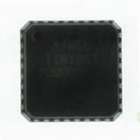
ATTINY861-20MU Atmel, ATTINY861-20MU Datasheet - Page 52

ATTINY861-20MU
Manufacturer Part Number
ATTINY861-20MU
Description
IC MCU AVR 8K FLASH 20MHZ 32-QFN
Manufacturer
Atmel
Series
AVR® ATtinyr
Specifications of ATTINY861-20MU
Core Processor
AVR
Core Size
8-Bit
Speed
20MHz
Connectivity
USI
Peripherals
Brown-out Detect/Reset, POR, PWM, WDT
Number Of I /o
16
Program Memory Size
8KB (4K x 16)
Program Memory Type
FLASH
Eeprom Size
512 x 8
Ram Size
512 x 8
Voltage - Supply (vcc/vdd)
2.7 V ~ 5.5 V
Data Converters
A/D 11x10b
Oscillator Type
Internal
Operating Temperature
-40°C ~ 85°C
Package / Case
32-VQFN Exposed Pad, 32-HVQFN, 32-SQFN, 32-DHVQFN
Processor Series
ATTINY8x
Core
AVR8
Data Bus Width
8 bit
Data Ram Size
512 B
Interface Type
2-Wire, SPI, USI
Maximum Clock Frequency
20 MHz
Number Of Programmable I/os
16
Number Of Timers
2
Maximum Operating Temperature
+ 85 C
Mounting Style
SMD/SMT
3rd Party Development Tools
EWAVR, EWAVR-BL
Development Tools By Supplier
ATAVRDRAGON, ATSTK500, ATSTK600, ATAVRISP2, ATAVRONEKIT, ATAVRMC320
Minimum Operating Temperature
- 40 C
On-chip Adc
10 bit, 11 Channel
Package
32MLF EP
Device Core
AVR
Family Name
ATtiny
Maximum Speed
20 MHz
Operating Supply Voltage
3.3|5 V
For Use With
ATSTK600 - DEV KIT FOR AVR/AVR32ATAVRBC100 - REF DESIGN KIT BATTERY CHARGER770-1007 - ISP 4PORT ATMEL AVR MCU SPI/JTAG
Lead Free Status / RoHS Status
Lead free / RoHS Compliant
Available stocks
Company
Part Number
Manufacturer
Quantity
Price
Company:
Part Number:
ATTINY861-20MU
Manufacturer:
LT
Quantity:
2 140
Part Number:
ATTINY861-20MU
Manufacturer:
ATMEL/爱特梅尔
Quantity:
20 000
9.3
9.3.1
9.3.2
52
Register Description
ATtiny261/461/861
MCUCR – MCU Control Register
GIMSK – General Interrupt Mask Register
rupt will be generated. The start-up time is defined by the SUT and CKSEL Fuses as described
in
If the low level on the interrupt pin is removed before the device has woken up then program
execution will not be diverted to the interrupt service routine but continue from the instruction fol-
lowing the SLEEP command.
The MCU Register contains control bits for interrupt sense control.
• Bits 1, 0 – ISC01, ISC00: Interrupt Sense Control 0 Bit 1 and Bit 0
The External Interrupt 0 is activated by the external pin INT0 or INT1 if the SREG I-flag and the
corresponding interrupt mask are set. The level and edges on the external INT0 or INT1 pin that
activate the interrupt are defined in
before detecting edges. If edge or toggle interrupt is selected, pulses that last longer than one
clock period will generate an interrupt. Shorter pulses are not guaranteed to generate an inter-
rupt. If low level interrupt is selected, the low level must be held until the completion of the
currently executing instruction to generate an interrupt.
Table 9-2.
• Bit 7 – INT1: External Interrupt Request 1 Enable
When the INT1 bit is set (one) and the I-bit in the Status Register (SREG) is set (one), the exter-
nal pin interrupt is enabled. The Interrupt Sense Control0 bits 1/0 (ISC01 and ISC00) in the MCU
Control Register (MCUCR) define whether the external interrupt is activated on rising and/or fall-
ing edge of the INT1 pin or level sensed. Activity on the pin will cause an interrupt request even
if INT1 is configured as an output. The corresponding interrupt of External Interrupt Request 1 is
executed from the INT1 Interrupt Vector.
• Bit 6 – INT0: External Interrupt Request 0 Enable
When the INT0 bit is set (one) and the I-bit in the Status Register (SREG) is set (one), the exter-
nal pin interrupt is enabled. The Interrupt Sense Control0 bits 1/0 (ISC01 and ISC00) in the MCU
Bit
0x35 (0x55)
Read/Write
Initial Value
Bit
0x3B (0x5B)
Read/Write
Initial Value
“Clock System” on page
ISC01
0
0
1
1
7
–
R
0
Interrupt 0 Sense Control
7
INT1
R/W
0
ISC00
0
1
0
1
6
PUD
R/W
0
6
INT0
R/W
0
Description
The low level of INT0 or INT1 generates an interrupt request.
Any logical change on INT0 or INT1 generates an interrupt request.
The falling edge of INT0 or INT1 generates an interrupt request.
The rising edge of INT0 or INT1 generates an interrupt request.
24.
5
SE
R/W
0
5
PCIE1
R/W
0
Table
4
SM1
R/W
0
4
PCIE0
R/w
0
9-2. The value on the INT0 or INT1 pin is sampled
3
SM0
R/W
0
3
–
R
0
2
–
R
0
2
–
R
0
1
ISC01
R/W
0
1
–
R
0
0
ISC00
0
R/W
0
–
R
0
2588E–AVR–08/10
MCUCR
GIMSK


