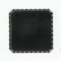
ATTINY861-20MU Atmel, ATTINY861-20MU Datasheet - Page 84

ATTINY861-20MU
Manufacturer Part Number
ATTINY861-20MU
Description
IC MCU AVR 8K FLASH 20MHZ 32-QFN
Manufacturer
Atmel
Series
AVR® ATtinyr
Specifications of ATTINY861-20MU
Core Processor
AVR
Core Size
8-Bit
Speed
20MHz
Connectivity
USI
Peripherals
Brown-out Detect/Reset, POR, PWM, WDT
Number Of I /o
16
Program Memory Size
8KB (4K x 16)
Program Memory Type
FLASH
Eeprom Size
512 x 8
Ram Size
512 x 8
Voltage - Supply (vcc/vdd)
2.7 V ~ 5.5 V
Data Converters
A/D 11x10b
Oscillator Type
Internal
Operating Temperature
-40°C ~ 85°C
Package / Case
32-VQFN Exposed Pad, 32-HVQFN, 32-SQFN, 32-DHVQFN
Processor Series
ATTINY8x
Core
AVR8
Data Bus Width
8 bit
Data Ram Size
512 B
Interface Type
2-Wire, SPI, USI
Maximum Clock Frequency
20 MHz
Number Of Programmable I/os
16
Number Of Timers
2
Maximum Operating Temperature
+ 85 C
Mounting Style
SMD/SMT
3rd Party Development Tools
EWAVR, EWAVR-BL
Development Tools By Supplier
ATAVRDRAGON, ATSTK500, ATSTK600, ATAVRISP2, ATAVRONEKIT, ATAVRMC320
Minimum Operating Temperature
- 40 C
On-chip Adc
10 bit, 11 Channel
Package
32MLF EP
Device Core
AVR
Family Name
ATtiny
Maximum Speed
20 MHz
Operating Supply Voltage
3.3|5 V
For Use With
ATSTK600 - DEV KIT FOR AVR/AVR32ATAVRBC100 - REF DESIGN KIT BATTERY CHARGER770-1007 - ISP 4PORT ATMEL AVR MCU SPI/JTAG
Lead Free Status / RoHS Status
Lead free / RoHS Compliant
Available stocks
Company
Part Number
Manufacturer
Quantity
Price
Company:
Part Number:
ATTINY861-20MU
Manufacturer:
LT
Quantity:
2 140
Part Number:
ATTINY861-20MU
Manufacturer:
ATMEL/爱特梅尔
Quantity:
20 000
11.10 Register Description
11.10.1
84
ATtiny261/461/861
TCCR0A – Timer/Counter0 Control Register A
• Bit 7 – TCW0: Timer/Counter0 Width
When this bit is written to one 16-bit mode is selected as described
Timer/Counter0 width is set to 16-bits and the Output Compare Registers OCR0A and OCR0B
are combined to form one 16-bit Output Compare Register. Because the 16-bit registers
TCNT0H/L and OCR0B/A are accessed by the AVR CPU via the 8-bit data bus, special proce-
dures must be followed. These procedures are described in section
bit Mode” on page
• Bit 6 – ICEN0: Input Capture Mode Enable
When this bit is written to onem, the Input Capture Mode is enabled.
• Bit 5 – ICNC0: Input Capture Noise Canceler
Setting this bit activates the Input Capture Noise Canceler. When the noise canceler is acti-
vated, the input from the Input Capture Pin (ICP0) is filtered. The filter function requires four
successive equal valued samples of the ICP0 pin for changing its output. The Input Capture is
therefore delayed by four System Clock cycles when the noise canceler is enabled.
• Bit 4 – ICES0: Input Capture Edge Select
This bit selects which edge on the Input Capture Pin (ICP0) that is used to trigger a capture
event. When the ICES0 bit is written to zero, a falling (negative) edge is used as trigger, and
when the ICES0 bit is written to one, a rising (positive) edge will trigger the capture. When a cap-
ture is triggered according to the ICES0 setting, the counter value is copied into the Input
Capture Register. The event will also set the Input Capture Flag (ICF0), and this can be used to
cause an Input Capture Interrupt, if this interrupt is enabled.
• Bit 3 - ACIC0: Analog Comparator Input Capture Enable
When written logic one, this bit enables the input capture function in Timer/Counter0 to be trig-
gered by the Analog Comparator. The comparator output is in this case directly connected to the
input capture front-end logic, making the comparator utilize the noise canceler and edge select
features of the Timer/Counter0 Input Capture interrupt. When written logic zero, no connection
between the Analog Comparator and the input capture function exists. To make the comparator
trigger the Timer/Counter0 Input Capture interrupt, the TICIE0 bit in the Timer Interrupt Mask
Register (TIMSK) must be set.
• Bits 2:1 – Res: Reserved Bits
These bits are reserved and will always read zero.
• Bit 0 – CTC0: Waveform Generation Mode
This bit controls the counting sequence of the counter, the source for maximum (TOP) counter
value, see
Normal mode (counter) and Clear Timer on Compare Match (CTC) mode (see
ation” on page
Bit
0x15 (0x35)
Read/Write
Initial Value
Figure 11-7 on page
77).
TCW0
R/W
7
0
80.
ICEN0
R/W
6
0
79. Modes of operation supported by the Timer/Counter unit are:
ICNC0
R/W
5
0
ICES0
R/W
4
0
ACIC0
R/W
3
0
R
2
0
–
“Accessing Registers in 16-
Figure 11-7 on page
R
1
–
0
“Modes of Oper-
CTC0
R/W
0
0
2588E–AVR–08/10
TCCR0A
79.


