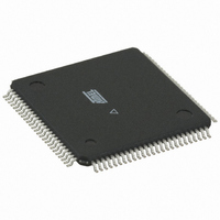
ATMEGA1280V-8AUR Atmel, ATMEGA1280V-8AUR Datasheet - Page 233

ATMEGA1280V-8AUR
Manufacturer Part Number
ATMEGA1280V-8AUR
Description
MCU AVR 128K FLASH 8MHZ 100TQFP
Manufacturer
Atmel
Series
AVR® ATmegar
Specifications of ATMEGA1280V-8AUR
Core Processor
AVR
Core Size
8-Bit
Speed
8MHz
Connectivity
EBI/EMI, I²C, SPI, UART/USART
Peripherals
Brown-out Detect/Reset, POR, PWM, WDT
Number Of I /o
86
Program Memory Size
128KB (64K x 16)
Program Memory Type
FLASH
Eeprom Size
4K x 8
Ram Size
8K x 8
Voltage - Supply (vcc/vdd)
1.8 V ~ 5.5 V
Data Converters
A/D 16x10b
Oscillator Type
Internal
Operating Temperature
-40°C ~ 85°C
Package / Case
100-TQFP, 100-VQFP
For Use With
ATSTK600-TQFP100 - STK600 SOCKET/ADAPTER 100-TQFPATSTK503 - STARTER KIT AVR EXP MODULE 100P
Lead Free Status / RoHS Status
Lead free / RoHS Compliant
Available stocks
Company
Part Number
Manufacturer
Quantity
Price
- Current page: 233 of 444
- Download datasheet (10Mb)
22.2.1
22.3
2549M–AVR–09/10
SPI Data Modes and Timing
Clock Generation
A comparison of the USART in MSPIM mode and the SPI pins is shown in
240.
The Clock Generation logic generates the base clock for the Transmitter and Receiver. For
USART MSPIM mode of operation only internal clock generation (that is, master operation) is
supported. The Data Direction Register for the XCKn pin (DDR_XCKn) must therefore be set to
one (that is, as output) for the USART in MSPIM to operate correctly. Preferably the DDR_XCKn
should be set up before the USART in MSPIM is enabled (that is, TXENn and RXENn bit set to
one).
The internal clock generation used in MSPIM mode is identical to the USART synchronous mas-
ter mode. The baud rate or UBRRn setting can therefore be calculated using the same
equations, see
Table 22-1.
Note:
There are four combinations of XCKn (SCK) phase and polarity with respect to serial data, which
are determined by control bits UCPHAn and UCPOLn. The data transfer timing diagrams are
shown in
the XCKn signal, ensuring sufficient time for data signals to stabilize. The UCPOLn and
UCPHAn functionality is summarized in
these bits will corrupt all ongoing communication for both the Receiver and Transmitter.
Table 22-2.
Operating Mode
Synchronous Master
mode
UCPOLn
BAUD
f
UBRRn
OSC
0
0
1
1
1. The baud rate is defined to be the transfer rate in bit per second (bps).
Figure 22-1 on page
Equations for Calculating Baud Rate Register Setting
UCPOLn and UCPHAn Functionality-
Table
UCPHAn
22-1.
Baud rate (in bits per second, bps).
System Oscillator clock frequency.
Contents of the UBRRnH and UBRRnL Registers, (0-4095).
0
1
0
1
Equation for Calculating Baud
BAUD
234. Data bits are shifted out and latched in on opposite edges of
ATmega640/1280/1281/2560/2561
=
SPI Mode
Rate
-------------------------------------- -
2 UBRRn
(
0
1
2
3
(1)
f
OSC
Table
+
22-2. Note that changing the setting of any of
1
)
Sample (Rising)
Sample (Falling)
Leading Edge
Setup (Rising)
Setup (Falling)
Equation for Calculating
UBRRn
UBRRn Value
=
------------------- - 1
2BAUD
f
OSC
Table 22-4 on page
Sample (Falling)
Sample (Rising)
Setup (Falling)
Setup (Rising)
Trailing Edge
–
233
Related parts for ATMEGA1280V-8AUR
Image
Part Number
Description
Manufacturer
Datasheet
Request
R

Part Number:
Description:
Manufacturer:
Atmel Corporation
Datasheet:

Part Number:
Description:
IC MCU AVR 128K FLASH 100-CBGA
Manufacturer:
Atmel
Datasheet:

Part Number:
Description:
IC MCU AVR 128K FLASH 100-TQFP
Manufacturer:
Atmel
Datasheet:

Part Number:
Description:
MCU AVR 128K FLASH 16MHZ 100TQFP
Manufacturer:
Atmel
Datasheet:

Part Number:
Description:
MCU AVR 128K FLASH 16MHZ 100CBGA
Manufacturer:
Atmel
Datasheet:

Part Number:
Description:
Manufacturer:
ATMEL Corporation
Datasheet:

Part Number:
Description:
Microcontroller with 128K bytes In-system programmable flash, 8 MHz, power supply =2.7 - 5.5V
Manufacturer:
ATMEL Corporation
Datasheet:

Part Number:
Description:
IC AVR MCU 128K 16MHZ 5V 64TQFP
Manufacturer:
Atmel
Datasheet:

Part Number:
Description:
IC AVR MCU 128K 16MHZ 5V 64-QFN
Manufacturer:
Atmel
Datasheet:

Part Number:
Description:
IC AVR MCU 128K 16MHZ COM 64-QFN
Manufacturer:
Atmel
Datasheet:

Part Number:
Description:
IC AVR MCU 128K 16MHZ 64-TQFP
Manufacturer:
Atmel
Datasheet:


