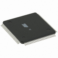
ATMEGA1280V-8AUR Atmel, ATMEGA1280V-8AUR Datasheet - Page 38

ATMEGA1280V-8AUR
Manufacturer Part Number
ATMEGA1280V-8AUR
Description
MCU AVR 128K FLASH 8MHZ 100TQFP
Manufacturer
Atmel
Series
AVR® ATmegar
Specifications of ATMEGA1280V-8AUR
Core Processor
AVR
Core Size
8-Bit
Speed
8MHz
Connectivity
EBI/EMI, I²C, SPI, UART/USART
Peripherals
Brown-out Detect/Reset, POR, PWM, WDT
Number Of I /o
86
Program Memory Size
128KB (64K x 16)
Program Memory Type
FLASH
Eeprom Size
4K x 8
Ram Size
8K x 8
Voltage - Supply (vcc/vdd)
1.8 V ~ 5.5 V
Data Converters
A/D 16x10b
Oscillator Type
Internal
Operating Temperature
-40°C ~ 85°C
Package / Case
100-TQFP, 100-VQFP
For Use With
ATSTK600-TQFP100 - STK600 SOCKET/ADAPTER 100-TQFPATSTK503 - STARTER KIT AVR EXP MODULE 100P
Lead Free Status / RoHS Status
Lead free / RoHS Compliant
Available stocks
Company
Part Number
Manufacturer
Quantity
Price
- Current page: 38 of 444
- Download datasheet (10Mb)
8.4.2
2549M–AVR–09/10
XMCRB – External Memory Control Register B
Figure 8-1 on page
external memory address space is treated as one sector. When the entire SRAM address space
is configured as one sector, the wait-states are configured by the SRW11 and SRW10 bits.
Table 8-2.
• Bit 3:2 – SRW11, SRW10: Wait-state Select Bits for Upper Sector
The SRW11 and SRW10 bits control the number of wait-states for the upper sector of the exter-
nal memory address space, see
• Bit 1:0 – SRW01, SRW00: Wait-state Select Bits for Lower Sector
The SRW01 and SRW00 bits control the number of wait-states for the lower sector of the exter-
nal memory address space, see
Table 8-3.
Note:
Bit
(0x75)
Read/Write
Initial Value
SRWn1
SRL2
0
0
1
1
0
0
0
1
1
1
1
1. n = 0 or 1 (lower/upper sector).
For further details of the timing and wait-states of the External Memory Interface, see Figures
8-3 through Figures 8-6 for how the setting of the SRW bits affects the timing.
SRWn0
XMBK
Sector limits with different settings of SRL2:0
Wait States
R/W
0
1
0
1
7
0
SRL1
28. By default, the SRL2, SRL1, and SRL0 bits are set to zero and the entire
0
1
1
0
0
1
1
Wait two cycles during read/write and wait one cycle before driving out new
R
6
–
0
(1)
SRL0
ATmega640/1280/1281/2560/2561
Table
Table
x
0
1
0
1
0
1
R
5
–
0
8-3.
8-3.
Wait two cycles during read/write strobe
Wait one cycle during read/write strobe
R
4
–
0
No wait-states
R
3
–
0
Wait States
Upper sector = 0xA000 - 0xFFFF
Upper sector = 0xC000 - 0xFFFF
Upper sector = 0xE000 - 0xFFFF
Upper sector = 0x2200 - 0xFFFF
Upper sector = 0x4000 - 0xFFFF
Upper sector = 0x6000 - 0xFFFF
Upper sector = 0x8000 - 0xFFFF
Lower sector = 0x2200 - 0xBFFF
Lower sector = 0x2200 - 0xDFFF
Lower sector = 0x2200 - 0x3FFF
Lower sector = 0x2200 - 0x5FFF
Lower sector = 0x2200 - 0x7FFF
Lower sector = 0x2200 - 0x9FFF
address
Lower sector = N/A
XMM2
R/W
Sector Limits
2
0
XMM1
R/W
1
0
XMM0
R/W
0
0
XMCRB
38
Related parts for ATMEGA1280V-8AUR
Image
Part Number
Description
Manufacturer
Datasheet
Request
R

Part Number:
Description:
Manufacturer:
Atmel Corporation
Datasheet:

Part Number:
Description:
IC MCU AVR 128K FLASH 100-CBGA
Manufacturer:
Atmel
Datasheet:

Part Number:
Description:
IC MCU AVR 128K FLASH 100-TQFP
Manufacturer:
Atmel
Datasheet:

Part Number:
Description:
MCU AVR 128K FLASH 16MHZ 100TQFP
Manufacturer:
Atmel
Datasheet:

Part Number:
Description:
MCU AVR 128K FLASH 16MHZ 100CBGA
Manufacturer:
Atmel
Datasheet:

Part Number:
Description:
Manufacturer:
ATMEL Corporation
Datasheet:

Part Number:
Description:
Microcontroller with 128K bytes In-system programmable flash, 8 MHz, power supply =2.7 - 5.5V
Manufacturer:
ATMEL Corporation
Datasheet:

Part Number:
Description:
IC AVR MCU 128K 16MHZ 5V 64TQFP
Manufacturer:
Atmel
Datasheet:

Part Number:
Description:
IC AVR MCU 128K 16MHZ 5V 64-QFN
Manufacturer:
Atmel
Datasheet:

Part Number:
Description:
IC AVR MCU 128K 16MHZ COM 64-QFN
Manufacturer:
Atmel
Datasheet:

Part Number:
Description:
IC AVR MCU 128K 16MHZ 64-TQFP
Manufacturer:
Atmel
Datasheet:


