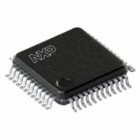
LPC2103FBD48,118 NXP Semiconductors, LPC2103FBD48,118 Datasheet - Page 9

LPC2103FBD48,118
Manufacturer Part Number
LPC2103FBD48,118
Description
IC ARM7 MCU FLASH 32K 48-LQFP
Manufacturer
NXP Semiconductors
Series
LPC2100r
Datasheet
1.LPC2102FHN48551.pdf
(37 pages)
Specifications of LPC2103FBD48,118
Core Processor
ARM7
Core Size
16/32-Bit
Speed
70MHz
Connectivity
I²C, Microwire, SPI, SSI, SSP, UART/USART
Peripherals
POR, PWM, WDT
Number Of I /o
32
Program Memory Size
32KB (32K x 8)
Program Memory Type
FLASH
Ram Size
8K x 8
Voltage - Supply (vcc/vdd)
1.65 V ~ 3.6 V
Data Converters
A/D 8x10b
Oscillator Type
Internal
Operating Temperature
-40°C ~ 85°C
Package / Case
48-LQFP
Processor Series
LPC21
Core
ARM7TDMI-S
Data Bus Width
32 bit
Data Ram Size
8 KB
Interface Type
I2C, JTAG, SPI, SSP, UART
Maximum Clock Frequency
70 MHz
Number Of Programmable I/os
32
Number Of Timers
4
Maximum Operating Temperature
+ 85 C
Mounting Style
SMD/SMT
3rd Party Development Tools
MDK-ARM, RL-ARM, ULINK2, DB-LQFP48-LPC2103, MCB2103, MCB2103U, MCB2103UME, KSK-LPC2103-01, KSK-LPC2103-01PL, KSK-LPC2103-02
Development Tools By Supplier
OM10079, OM10081, OM10090
Minimum Operating Temperature
- 40 C
On-chip Adc
10 bit, 8 Channel
For Use With
568-4302 - BOARD EVAL LPC210X KS2103 JLINK568-4301 - BOARD EVAL LPC210X KS2103568-4300 - BOARD EVAL LPC210X MCB2103568-4297 - BOARD EVAL LPC21XX MCB2100MCB2103UME - BOARD EVAL MCB2103 + ULINK-MEMCB2103U - BOARD EVAL MCB2103 + ULINK2622-1013 - BOARD FOR LPC2103 48-LQFP622-1008 - BOARD FOR LPC9103 10-HVSONMCB2103 - BOARD EVAL NXP LPC2101/2101/2103
Lead Free Status / RoHS Status
Lead free / RoHS Compliant
Eeprom Size
-
Lead Free Status / Rohs Status
Details
Other names
935280966118
LPC2103FBD48-T
LPC2103FBD48-T
LPC2103FBD48-T
LPC2103FBD48-T
Available stocks
Company
Part Number
Manufacturer
Quantity
Price
Company:
Part Number:
LPC2103FBD48,118
Manufacturer:
NXP Semiconductors
Quantity:
10 000
NXP Semiconductors
Table 3.
[1]
[2]
[3]
[4]
[5]
[6]
[7]
[8]
[9]
LPC2101_02_03_4
Product data sheet
Symbol
V
V
V
V
V
VBAT
SS
SSA
DDA
DD(1V8)
DD(3V3)
5 V tolerant (if V
Open-drain 5 V tolerant (if V
pull-up to provide an output functionality. Open-drain configuration applies to ALL functions on that pin.
5 V tolerant (if V
analog input function. If configured for an input function, this pad utilizes built-in glitch filter that blocks pulses shorter than 3 ns. When
configured as an ADC input, digital section of the pad is disabled.
5 V tolerant (if V
If configured for an input function, this pad utilizes built-in glitch filter that blocks pulses shorter than 3 ns.
A LOW level during reset on pin P0.14 is considered as an external hardware request to start the ISP command handler.
Open-drain 5 V tolerant (if V
pull-up to provide an output functionality. Open-drain configuration applies only to I
Pad provides special analog functionality.
For lowest power consumption, pin should be left floating when the RTC is not used.
See LPC2101/02/03 User manual UM10161 for details.
Pin description
Pin
7, 19, 43
31
42
5
17, 40
4
DD(3V3)
DD(3V3)
DD(3V3)
and V
and V
and V
…continued
DD(3V3)
DD(3V3)
DDA
DDA
DDA
Type
I
I
I
I
I
I
3.0 V) pad providing digital I/O functions with TTL levels and hysteresis and 10 ns slew rate control.
3.0 V) pad providing digital I/O functions with TTL levels and hysteresis and 10 ns slew rate control.
and V
3.0 V) pad providing digital I/O (with TTL levels and hysteresis and 10 ns slew rate control) and
and V
DDA
DDA
Description
Ground: 0 V reference.
Analog ground: 0 V reference. This should be nominally the same voltage as
V
Analog 3.3 V power supply: This should be nominally the same voltage as
V
pin also provides a voltage reference level for the ADC.
1.8 V core power supply: This is the power supply voltage for internal
circuitry and the on-chip PLL.
3.3 V pad power supply: This is the power supply voltage for the I/O ports.
RTC power supply: 3.3 V on this pin supplies the power to the RTC.
3.0 V) digital I/O I
3.0 V) digital I/O I
SS
DD(3V3)
but should be isolated to minimize noise and error.
Rev. 04 — 2 June 2009
but should be isolated to minimize noise and error. The level on this
2
2
C-bus 400 kHz specification compatible pad. It requires external
C-bus 400 kHz specification compatible pad. It requires external
Single-chip 16-bit/32-bit microcontrollers
2
C function on that pin.
LPC2101/02/03
© NXP B.V. 2009. All rights reserved.
9 of 37


