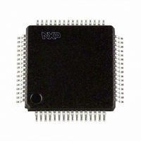
P89LPC9408FBD,557 NXP Semiconductors, P89LPC9408FBD,557 Datasheet - Page 21

P89LPC9408FBD,557
Manufacturer Part Number
P89LPC9408FBD,557
Description
IC 80C51 MCU FLASH 8K 64-LQFP
Manufacturer
NXP Semiconductors
Series
LPC900r
Datasheet
1.P89LPC9408FBD557.pdf
(69 pages)
Specifications of P89LPC9408FBD,557
Program Memory Type
FLASH
Program Memory Size
8KB (8K x 8)
Package / Case
64-LQFP
Core Processor
8051
Core Size
8-Bit
Speed
18MHz
Connectivity
I²C, SPI, UART/USART
Peripherals
Brown-out Detect/Reset, LCD, LED, POR, PWM, WDT
Number Of I /o
23
Eeprom Size
512 x 8
Ram Size
256 x 8
Voltage - Supply (vcc/vdd)
2.4 V ~ 3.6 V
Data Converters
A/D 8x10b
Oscillator Type
Internal
Operating Temperature
-40°C ~ 85°C
Processor Series
P89LPC9x
Core
80C51
Data Bus Width
8 bit
Data Ram Size
256 B
Interface Type
I2C/SPI/UART
Maximum Clock Frequency
18 MHz
Number Of Programmable I/os
23
Number Of Timers
2
Operating Supply Voltage
2.4 V to 3.6 V
Maximum Operating Temperature
+ 85 C
Mounting Style
SMD/SMT
3rd Party Development Tools
PK51, CA51, A51, ULINK2
Minimum Operating Temperature
- 40 C
On-chip Adc
8-ch x 10-bit
Lead Free Status / RoHS Status
Lead free / RoHS Compliant
For Use With
OM10097 - KIT FOR LCD DEMO LPC9408EPM900K - EMULATOR/PROGRAMMER NXP P89LPC9568-4000 - DEMO BOARD SPI/I2C TO DUAL UART568-3510 - DEMO BOARD SPI/I2C TO UART568-1759 - EMULATOR DEBUGGER/PROGRMMR LPC9X
Lead Free Status / Rohs Status
Lead free / RoHS Compliant
Other names
568-3228
935280583557
P89LPC9408FBD
935280583557
P89LPC9408FBD
Available stocks
Company
Part Number
Manufacturer
Quantity
Price
Company:
Part Number:
P89LPC9408FBD,557
Manufacturer:
NXP Semiconductors
Quantity:
10 000
Philips Semiconductors
P89LPC9408_1
Product data sheet
7.7 CPU Clock (CCLK) wake-up delay
7.8 CCLK modification: DIVM register
7.9 Low power select
The P89LPC9408 has an internal wake-up timer that delays the clock until it stabilizes
depending on the clock source used. If the clock source is any of the three crystal
selections (low, medium and high frequencies) the delay is 992 OSCCLK cycles plus
60 s to 100 s. If the clock source is either the internal RC oscillator, watchdog oscillator,
or external clock, the delay is 224 OSCCLK cycles plus 60 s to 100 s.
The OSCCLK frequency can be divided down up to 510 times by configuring a dividing
register, DIVM, to generate CCLK. This feature makes it possible to temporarily run the
CPU at a lower rate, reducing power consumption. By dividing the clock, the CPU can
retain the ability to respond to events that would not exit Idle mode by executing its normal
program at a lower rate. This can also allow bypassing the oscillator start-up time in cases
where Power-down mode would otherwise be used. The value of DIVM may be changed
by the program at any time without interrupting code execution.
The P89LPC9408 is designed to run at 18 MHz (CCLK) maximum. However, if CCLK is
8 MHz or slower, the CLKLP SFR bit (AUXR1.7) can be set to logic 1 to lower the power
consumption further. On any reset, CLKLP is logic 0 allowing highest performance
access. This bit can then be set in software if CCLK is running at 8 MHz or slower.
Fig 6. Block diagram of oscillator control
XTAL1
XTAL2
(400 kHz 30 % 20 %)
(7.3728 MHz
OSCILLATOR
OSCILLATOR
WATCHDOG
RC
8-bit two-clock 80C51 core with 32 segment
MEDIUM FREQUENCY
HIGH FREQUENCY
LOW FREQUENCY
1 %)
Rev. 01 — 16 December 2005
TIMER 0 AND
RCCLK
TIMER 1
I
2
C-BUS
OSCCLK
PCLK
DIVM
SPI
CCLK
PCLK
© Koninklijke Philips Electronics N.V. 2005. All rights reserved.
2
UART
P89LPC9408
4 LCD driver, 10-bit ADC
ADC0
WDT
RTC
CPU
32
CCU
PLL
002aab102
21 of 69


