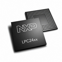
LPC2468FET208,551 NXP Semiconductors, LPC2468FET208,551 Datasheet - Page 22

LPC2468FET208,551
Manufacturer Part Number
LPC2468FET208,551
Description
IC ARM7 MCU FLASH 512K 208TFBGA
Manufacturer
NXP Semiconductors
Series
LPC2400r
Specifications of LPC2468FET208,551
Program Memory Type
FLASH
Program Memory Size
512KB (512K x 8)
Package / Case
208-TFBGA
Core Processor
ARM7
Core Size
16/32-Bit
Speed
72MHz
Connectivity
CAN, EBI/EMI, Ethernet, I²C, Microwire, MMC, SPI, SSI, SSP, UART/USART, USB OTG
Peripherals
Brown-out Detect/Reset, DMA, I²S, POR, PWM, WDT
Number Of I /o
160
Ram Size
98K x 8
Voltage - Supply (vcc/vdd)
3 V ~ 3.6 V
Data Converters
A/D 8x10b; D/A 1x10b
Oscillator Type
Internal
Operating Temperature
-40°C ~ 85°C
Processor Series
LPC24
Core
ARM7TDMI-S
Data Bus Width
16 bit, 32 bit
Data Ram Size
98 KB
Interface Type
CAN/I2S/ISP/SSP/UART/USB
Maximum Clock Frequency
72 MHz
Number Of Programmable I/os
160
Number Of Timers
6
Operating Supply Voltage
3.3 V
Maximum Operating Temperature
+ 85 C
Mounting Style
SMD/SMT
3rd Party Development Tools
MDK-ARM, RL-ARM, ULINK2, IRD-LPC2468-DEV, SAB-TFBGA208, KSK-LPC2468-PL
Development Tools By Supplier
OM10100
Minimum Operating Temperature
- 40 C
On-chip Adc
8-ch x 10-bit
On-chip Dac
1-ch x 10-bit
Package
208TFBGA
Device Core
ARM7TDMI-S
Family Name
LPC2000
Maximum Speed
72 MHz
Lead Free Status / RoHS Status
Lead free / RoHS Compliant
For Use With
622-1025 - KIT DEV IND REF DESIGN LPC2468622-1024 - BOARD SCKT ADAPTER FOR TFBGA208568-4358 - DISPLAY QVGA TFT FOR OM10100568-4309 - BOARD EXTENSION LPCSTICK568-4308 - EVAL LPC-STICK WITH LPC2468MCB2400U - BOARD EVAL MCB2400 + ULINK2MCB2400 - BOARD EVAL FOR NXP LPC246X SER622-1005 - USB IN-CIRCUIT PROG ARM7 LPC2K
Eeprom Size
-
Lead Free Status / Rohs Status
Lead free / RoHS Compliant
Other names
568-4262
935283234551
LPC2468FET208-S
935283234551
LPC2468FET208-S
Available stocks
Company
Part Number
Manufacturer
Quantity
Price
Company:
Part Number:
LPC2468FET208,551
Manufacturer:
NXP
Quantity:
6 174
Company:
Part Number:
LPC2468FET208,551
Manufacturer:
NXP Semiconductors
Quantity:
10 000
NXP Semiconductors
Table 4.
LPC2468
Product data sheet
Symbol
P4[29]/BLS3/
MAT2[1]/RXD3
P4[30]/CS0
P4[31]/CS1
ALARM
USB_D−2
DBGEN
TDO
TDI
TMS
TRST
TCK
RTCK
RSTOUT
RESET
XTAL1
XTAL2
RTCX1
RTCX2
V
V
V
SSIO
SSCORE
SSA
Pin description
Pin
176
187
193
37
52
9
2
4
6
8
10
206
29
35
44
46
34
36
33, 63,
77, 93,
114,
133,
148,
169,
189,
200
32, 84,
172
22
[1][8]
[1][9]
[1][8]
[1][8]
[1][8]
[7]
[1][9]
[1]
[10]
[7][11]
[7][11]
[7][12]
[7][12]
[14]
[1]
[1]
[1]
[1][8]
[13]
[13]
…continued
Ball
B10
B7
A4
N1
U1
F4
D3
C2
E3
D1
E2
C3
K3
M2
M4
N4
K2
L2
L3, T5,
R9, P12,
N16,
H14,
E15,
A12, B6,
A2
K4, P10,
D12
J2
[14]
[7][12]
[1][8]
[1]
[1]
[1][8]
[1][9]
[1]
[7][12]
[13]
[7]
[1][9]
[1][8]
[1][8]
[1][8]
[7][11]
[10]
[7][11]
[1]
[13]
All information provided in this document is subject to legal disclaimers.
Type
I/O
O
O
I
I/O
O
I/O
O
O
I/O
I
O
I
I
I
I
I/O
O
I
I
O
I
O
I
I
I
Rev. 5 — 15 October 2010
Description
P4[29] — General purpose digital input/output pin.
BLS3 — LOW active Byte Lane select signal 3.
MAT2[1] — Match output for Timer 2, channel 1.
RXD3 — Receiver input for UART3.
P4[30] — General purpose digital input/output pin.
CS0 — LOW active Chip Select 0 signal.
P4[31] — General purpose digital input/output pin.
CS1 — LOW active Chip Select 1 signal.
ALARM — RTC controlled output. This is a 1.8 V pin. It goes HIGH when
a RTC alarm is generated.
USB_D−2 — USB port 2 bidirectional D− line.
DBGEN — JTAG interface control signal. Also used for boundary
scanning.
TDO — Test Data Out for JTAG interface.
TDI — Test Data In for JTAG interface.
TMS — Test Mode Select for JTAG interface.
TRST — Test Reset for JTAG interface.
TCK — Test Clock for JTAG interface. This clock must be slower than
of the CPU clock (CCLK) for the JTAG interface to operate.
RTCK — JTAG interface control signal.
Note: LOW on this pin while RESET is LOW enables ETM pins (P2[9:0])
to operate as Trace port after reset.
RSTOUT — This is a 3.3 V pin. LOW on this pin indicates LPC2468
being in Reset state.
external reset input: A LOW on this pin resets the device, causing I/O
ports and peripherals to take on their default states, and processor
execution to begin at address 0. TTL with hysteresis, 5 V tolerant.
Input to the oscillator circuit and internal clock generator circuits.
Output from the oscillator amplifier.
Input to the RTC oscillator circuit.
Output from the RTC oscillator circuit.
ground: 0 V reference for the digital I/O pins.
ground: 0 V reference for the core.
analog ground: 0 V reference. This should nominally be the same
voltage as V
error.
SSIO
/V
SSCORE
, but should be isolated to minimize noise and
Single-chip 16-bit/32-bit micro
LPC2468
© NXP B.V. 2010. All rights reserved.
22 of 85
1
⁄
6


