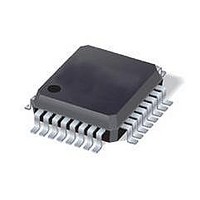
ST7FLI49MK1T6 STMicroelectronics, ST7FLI49MK1T6 Datasheet - Page 72

ST7FLI49MK1T6
Manufacturer Part Number
ST7FLI49MK1T6
Description
MCU 8BIT SGL VOLT FLASH 32-LQFP
Manufacturer
STMicroelectronics
Series
ST7r
Datasheet
1.ST7FLI49MK1T6TR.pdf
(187 pages)
Specifications of ST7FLI49MK1T6
Core Processor
ST7
Core Size
8-Bit
Speed
8MHz
Connectivity
I²C
Peripherals
LVD, POR, PWM, WDT
Number Of I /o
24
Program Memory Size
4KB (4K x 8)
Program Memory Type
FLASH
Eeprom Size
128 x 8
Ram Size
384 x 8
Voltage - Supply (vcc/vdd)
2.4 V ~ 5.5 V
Data Converters
A/D 10x10b
Oscillator Type
Internal
Operating Temperature
-40°C ~ 85°C
Package / Case
32-LQFP
Processor Series
ST7FLI4x
Core
ST7
Data Bus Width
8 bit
Data Ram Size
384 B
Interface Type
I2C
Maximum Clock Frequency
8 MHz
Number Of Programmable I/os
24
Number Of Timers
5
Maximum Operating Temperature
+ 125 C
Mounting Style
SMD/SMT
Minimum Operating Temperature
- 40 C
On-chip Adc
10 bit, 10 Channel
Lead Free Status / RoHS Status
Lead free / RoHS Compliant
Available stocks
Company
Part Number
Manufacturer
Quantity
Price
Company:
Part Number:
ST7FLI49MK1T6
Manufacturer:
st
Quantity:
456
Company:
Part Number:
ST7FLI49MK1T6
Manufacturer:
STMicroelectronics
Quantity:
10 000
Part Number:
ST7FLI49MK1T6
Manufacturer:
ST
Quantity:
20 000
Company:
Part Number:
ST7FLI49MK1T6TR
Manufacturer:
STMicroelectronics
Quantity:
10 000
I/O ports
10.2.4
Caution:
10.3
10.4
10.5
72/188
Analog alternate function
Configure the I/O as floating input to use an ADC input. The analog multiplexer (controlled
by the ADC registers) switches the analog voltage present on the selected pin to the
common analog rail, connected to the ADC input.
Analog Recommendations
Do not change the voltage level or loading on any I/O while conversion is in progress. Do not
have clocking pins located close to a selected analog pin.
The analog input voltage level must be within the limits stated in the absolute maximum
ratings.
I/O port implementation
The hardware implementation on each I/O port depends on the settings in the DDR and OR
registers and specific I/O port features such as ADC input or open-drain.
Switching these I/O ports from one state to another should be done in a sequence that
prevents unwanted side effects. Recommended safe transitions are illustrated in
Other transitions are potentially risky and should be avoided, since they may present
unwanted side-effects such as spurious interrupt generation.
Figure 35. Interrupt I/O port state transitions
Unused I/O pins
Unused I/O pins must be connected to fixed voltage levels. Refer to
pin
Low power modes
Table 26.
s
characteristics.
Mode
Wait
Halt
Effect of low power modes on I/O ports
No effect on I/O ports. External interrupts cause the device to exit from Wait
No effect on I/O ports. External interrupts cause the device to exit from Halt
floating/pull-up
interrupt
INPUT
01
Doc ID 13562 Rev 3
(reset state)
floating
INPUT
00
open-drain
OUTPUT
XX
Description
10
mode.
mode.
= DDR, OR
OUTPUT
push-pull
11
Section 13.9: I/O port
ST7LITE49M
Figure
35.


