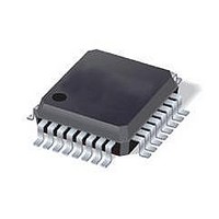
ST7FLI49MK1T6 STMicroelectronics, ST7FLI49MK1T6 Datasheet - Page 96

ST7FLI49MK1T6
Manufacturer Part Number
ST7FLI49MK1T6
Description
MCU 8BIT SGL VOLT FLASH 32-LQFP
Manufacturer
STMicroelectronics
Series
ST7r
Datasheet
1.ST7FLI49MK1T6TR.pdf
(187 pages)
Specifications of ST7FLI49MK1T6
Core Processor
ST7
Core Size
8-Bit
Speed
8MHz
Connectivity
I²C
Peripherals
LVD, POR, PWM, WDT
Number Of I /o
24
Program Memory Size
4KB (4K x 8)
Program Memory Type
FLASH
Eeprom Size
128 x 8
Ram Size
384 x 8
Voltage - Supply (vcc/vdd)
2.4 V ~ 5.5 V
Data Converters
A/D 10x10b
Oscillator Type
Internal
Operating Temperature
-40°C ~ 85°C
Package / Case
32-LQFP
Processor Series
ST7FLI4x
Core
ST7
Data Bus Width
8 bit
Data Ram Size
384 B
Interface Type
I2C
Maximum Clock Frequency
8 MHz
Number Of Programmable I/os
24
Number Of Timers
5
Maximum Operating Temperature
+ 125 C
Mounting Style
SMD/SMT
Minimum Operating Temperature
- 40 C
On-chip Adc
10 bit, 10 Channel
Lead Free Status / RoHS Status
Lead free / RoHS Compliant
Available stocks
Company
Part Number
Manufacturer
Quantity
Price
Company:
Part Number:
ST7FLI49MK1T6
Manufacturer:
st
Quantity:
456
Company:
Part Number:
ST7FLI49MK1T6
Manufacturer:
STMicroelectronics
Quantity:
10 000
Part Number:
ST7FLI49MK1T6
Manufacturer:
ST
Quantity:
20 000
Company:
Part Number:
ST7FLI49MK1T6TR
Manufacturer:
STMicroelectronics
Quantity:
10 000
On-chip peripherals
96/188
Bit 6 = BREDGE Break input edge selection bit
Bit 5 = BA Break active bit
Bit 4 = BPEN Break pin enable bit
Bits 3:0 = PWM[3:0] Break pattern bits
PWMx duty cycle register High (DCRxH)
Reset value: 0000 0000 (00h)
Bits 15:12 = Reserved.
PWMx duty cycle register Low (DCRxL)
Reset value: 0000 0000 (00h)
Bits 11:0 = DCRx[11:0] PWMx duty cycle value: this 12-bit value is written by software. It
defines the duty cycle of the corresponding PWM output signal (see
In PWM mode (OEx=1 in the PWMCR register) the DCR[11:0] bits define the duty cycle of
the PWMx output signal (see
be compared with the 12-bit upcounter value.
DCR7
15
This bit is read/write by software and cleared by hardware after reset. It selects the
active level of Break signal.
0: Low level of Break selected as active level
1: High level of Break selected as active level
This bit is read/write by software, cleared by hardware after reset and set by hardware
when the active level defined by the BR1EDGE bit is applied on the BREAK pin. It
activates/deactivates the Break function.
0: Break not active
1: Break active
This bit is read/write by software and cleared by hardware after reset.
0: Break pin disabled
1: Break pin enabled
These bits are read/write by software and cleared by hardware after a reset. They are
used to force the four PWMx output signals into a stable state when the Break function
is active and corresponding OEx bit is set.
0
7
DCR6
0
DCR5
0
Figure
Doc ID 13562 Rev 3
40). In output compare mode, they define the value to
DCR4
0
Read/write
Read/write
DCR11
DCR3
DCR10
DCR2
Figure
DCR1
DCR9
40).
ST7LITE49M
DCR0
DCR8
0
8


