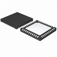
ST72F63BK2U1TR STMicroelectronics, ST72F63BK2U1TR Datasheet - Page 151

ST72F63BK2U1TR
Manufacturer Part Number
ST72F63BK2U1TR
Description
IC MCU 8BIT 8K FLASH 40-QFN
Manufacturer
STMicroelectronics
Series
ST7r
Datasheet
1.ST72F63BD6U1TR.pdf
(186 pages)
Specifications of ST72F63BK2U1TR
Core Processor
ST7
Core Size
8-Bit
Speed
8MHz
Connectivity
I²C, SCI, USB
Peripherals
DMA, LVD, POR, PWM, WDT
Number Of I /o
19
Program Memory Size
8KB (8K x 8)
Program Memory Type
FLASH
Ram Size
384 x 8
Voltage - Supply (vcc/vdd)
4 V ~ 5.5 V
Data Converters
A/D 12x8b
Oscillator Type
External
Operating Temperature
0°C ~ 70°C
Package / Case
40-QFN
Processor Series
ST72F6x
Core
ST7
Data Bus Width
8 bit
Data Ram Size
384 B
Interface Type
I2C, SCI
Maximum Clock Frequency
8 MHz
Number Of Programmable I/os
19
Number Of Timers
2
Maximum Operating Temperature
+ 70 C
Mounting Style
SMD/SMT
Development Tools By Supplier
ST7MDTU3-EPB/US, ST72F63B-SK/RAIS, ST7MDTU3-EMU3, STX-RLINK
Minimum Operating Temperature
0 C
On-chip Adc
8 bit, 8 Channel / 8 bit, 12 Channel
Lead Free Status / RoHS Status
Lead free / RoHS Compliant
Eeprom Size
-
Lead Free Status / Rohs Status
Details
Available stocks
Company
Part Number
Manufacturer
Quantity
Price
- Current page: 151 of 186
- Download datasheet (3Mb)
ST7263Bxx
Table 71.
1. The I
2. The I
3. The minimum V
Symbol
V
V
ports and control pins) must not exceed I
ports and control pins) must not exceed I
for ROM devices, min = V
OH
OL
(1)
(2)
IO
IO
current sourced must always respect the absolute maximum rating specified in
current sunk must always respect the absolute maximum rating specified in
Output low level voltage for a standard I/O pin
when up to 8 pins are sunk at the same time,
Port A0, Port A(3:7), Port C(0:2), Port D(0:7)
Output low level voltage for a high sink I/O pin
when up to 4 pins are sunk at the same time,
Port B(0:7)
Output low level voltage for a very high sink I/O
pin when up to 2 pins are sunk at the same
time, Port A1, Port A2
Output high level voltage for an I/O pin
when up to 8 pins are sourced at same time
Output driving current
Figure 63. V
OH
value (with I
DD
- 1.7 V
Parameter
OL
IO
=-10mA) depends on the chosen device type. For Flash devices, min = V
standard V
250
200
150
100
50
0
1
VSS
VDD
.
. True open drain I/O pins does not have V
DD
1.5
Doc ID 7516 Rev 8
=5 V
Vol_2mA (mV) at Vdd=5V
2
Iio (mA)
2.5
Conditions
I
I
I
I
I
IO
IO
IO
IO
IO
=+1.6 mA
=+10 mA
=+25 mA
=-10 mA
=-1.6 mA
3
Section 13.2
Section 13.2
OH
.
Electrical characteristics
V
3.5
V
DD
DD
and the sum of I
Min
-1.3
-
-
-
and the sum of I
-0.8
ai15597
(3)
4
DD
Max
0.4
1.3
1.5
- 1.3 V and
-
-
IO
IO
(I/O
151/186
(I/O
Unit
V
Related parts for ST72F63BK2U1TR
Image
Part Number
Description
Manufacturer
Datasheet
Request
R

Part Number:
Description:
KIT STARTER LOW COST ST7
Manufacturer:
STMicroelectronics
Datasheet:

Part Number:
Description:
STMicroelectronics [RIPPLE-CARRY BINARY COUNTER/DIVIDERS]
Manufacturer:
STMicroelectronics
Datasheet:

Part Number:
Description:
STMicroelectronics [LIQUID-CRYSTAL DISPLAY DRIVERS]
Manufacturer:
STMicroelectronics
Datasheet:

Part Number:
Description:
BOARD EVAL FOR MEMS SENSORS
Manufacturer:
STMicroelectronics
Datasheet:

Part Number:
Description:
NPN TRANSISTOR POWER MODULE
Manufacturer:
STMicroelectronics
Datasheet:

Part Number:
Description:
TURBOSWITCH ULTRA-FAST HIGH VOLTAGE DIODE
Manufacturer:
STMicroelectronics
Datasheet:

Part Number:
Description:
Manufacturer:
STMicroelectronics
Datasheet:

Part Number:
Description:
DIODE / SCR MODULE
Manufacturer:
STMicroelectronics
Datasheet:

Part Number:
Description:
DIODE / SCR MODULE
Manufacturer:
STMicroelectronics
Datasheet:

Part Number:
Description:
Search -----> STE16N100
Manufacturer:
STMicroelectronics
Datasheet:

Part Number:
Description:
Search ---> STE53NA50
Manufacturer:
STMicroelectronics
Datasheet:

Part Number:
Description:
NPN Transistor Power Module
Manufacturer:
STMicroelectronics
Datasheet:


