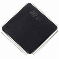
ST10R272LT6 STMicroelectronics, ST10R272LT6 Datasheet - Page 40

ST10R272LT6
Manufacturer Part Number
ST10R272LT6
Description
IC MCU 16BIT LV ROMLESS 100-TQFP
Manufacturer
STMicroelectronics
Series
ST10r
Datasheet
1.ST10R272LT1TR.pdf
(77 pages)
Specifications of ST10R272LT6
Core Processor
ST10
Core Size
16-Bit
Speed
50MHz
Connectivity
EBI/EMI, SSP, UART/USART
Peripherals
POR, PWM, WDT
Number Of I /o
77
Program Memory Type
ROMless
Ram Size
1K x 8
Voltage - Supply (vcc/vdd)
3 V ~ 3.6 V
Oscillator Type
Internal
Operating Temperature
-40°C ~ 85°C
Package / Case
144-TQFP, 144-VQFP
Processor Series
ST10R2x
Core
ST10
Data Bus Width
16 bit
Data Ram Size
1 KB
Interface Type
SSP, USART
Maximum Clock Frequency
50 MHz
Number Of Programmable I/os
77
Number Of Timers
5
Maximum Operating Temperature
+ 85 C
Mounting Style
SMD/SMT
Minimum Operating Temperature
- 40 C
On-chip Adc
16 bit
Lead Free Status / RoHS Status
Contains lead / RoHS non-compliant
Eeprom Size
-
Program Memory Size
-
Data Converters
-
Lead Free Status / Rohs Status
In Transition
Other names
497-2045
Available stocks
Company
Part Number
Manufacturer
Quantity
Price
Company:
Part Number:
ST10R272LT6
Manufacturer:
CYPRESS
Quantity:
1 400
Company:
Part Number:
ST10R272LT6
Manufacturer:
STMicroelectronics
Quantity:
10 000
Part Number:
ST10R272LT6
Manufacturer:
ST
Quantity:
20 000
ST10R272L - ELECTRICAL CHARACTERISTICS
16
16.1 Absolute Maximum Ratings
•
•
•
•
•
•
•
•
•
Note
The parameters listed in this section represent both the ST10R272L controller characteristics
and the system requirements. To aid parameters interpretation in design evaluation, the a
symbol column is marked:
40/77
1
CC for Controller Characteristics: The ST10R272L logic provides signals with the
SR for System Requirement:
Ambient temperature under bias ( T
Storage temperature ( T
Voltage on V
Voltage on any pin with respect to ground ( V
Voltage on any 5V tolerant pin with respect to ground ( V
Voltage on any 5V fail-safe pin with respect to ground ( V
Input current on any pin during overload condition: .................................. –10 to +10 mA
Absolute sum of all input currents during overload condition: .............................|100 mA|
Power dissipation:.....................................................................................................1.0 W
ELECTRICAL CHARACTERISTICS
Stresses above those listed under “Absolute Maximum Ratings” may cause
permanent damage to the device. This is a stress rating only and functional
operation of the device at these or any other conditions above those indicated in the
operational sections of this specification is not guaranteed. Exposure to absolute
maximum rating conditions for extended periods may affect device reliability. During
overload conditions (V
(V
SS
) must not exceed the values defined by the Absolute Maximum Ratings.
DD
pins with respect to ground ( V
ST
):....................................................................... – 65 to +150 °C
IN
>V
respective timing characteristics.
The external system must provide signals with the
respective timing characteristics to the ST10R272L.
DD
A
or V
): ......................................................... -40 to +85 °C
IN
<V
SS
SS
SS
) the voltage on pins with respect to ground
): ................................ –0.5 to V
):..................................... – 0.5 to +4.0 V
SS
SS
): .......................–0.5 to 5 .5 V
): .......................–0.5 to 5 .5 V
DD
+0.5 V


