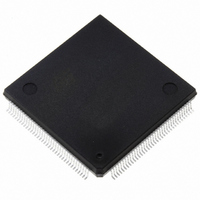
ST10F269Z2Q6/TR STMicroelectronics, ST10F269Z2Q6/TR Datasheet - Page 145

ST10F269Z2Q6/TR
Manufacturer Part Number
ST10F269Z2Q6/TR
Description
MCU 16BIT 256KBIT FLASH 144-PQFP
Manufacturer
STMicroelectronics
Series
ST10r
Datasheet
1.ST10F269Z2Q3.pdf
(184 pages)
Specifications of ST10F269Z2Q6/TR
Core Processor
ST10
Core Size
16-Bit
Speed
40MHz
Connectivity
CAN, EBI/EMI, SSC, UART/USART
Peripherals
POR, PWM, WDT
Number Of I /o
111
Program Memory Size
256KB (256K x 8)
Program Memory Type
FLASH
Ram Size
12K x 8
Voltage - Supply (vcc/vdd)
4.5 V ~ 5.5 V
Data Converters
A/D 16x10b
Oscillator Type
Internal
Operating Temperature
-40°C ~ 85°C
Package / Case
144-QFP
Processor Series
ST10F26x
Core
ST10
Data Bus Width
16 bit
Data Ram Size
12 KB
Interface Type
CAN, SSC, USART
Maximum Clock Frequency
40 MHz
Number Of Programmable I/os
111
Number Of Timers
5
Maximum Operating Temperature
+ 85 C
Mounting Style
SMD/SMT
Minimum Operating Temperature
- 40 C
On-chip Adc
10 bit, 16 Channel
Lead Free Status / RoHS Status
Lead free / RoHS Compliant
Eeprom Size
-
Lead Free Status / Rohs Status
Details
Available stocks
Company
Part Number
Manufacturer
Quantity
Price
Company:
Part Number:
ST10F269Z2Q6/TR
Manufacturer:
STMicroelectronics
Quantity:
10 000
ST10F269
21.3.2 - Conversion Timing Control
When
capacitances of the converter are loaded via the
respective analog input pin to the current analog
input voltage. The time to load the capacitances is
referred to as the sample time t
sampled voltage is converted to a digital value in
10 successive steps, which correspond to the
10-bit resolution of the ADC. The next 4 steps are
used for equalizing internal levels (and are kept for
exact timing matching with the 10-bit A/D
converter module implemented in the ST10F168).
The current that has to be drawn from the sources
for sampling and changing charges depends on
the time that each respective step takes, because
the capacitors must reach their final voltage level
within the given time, at least with a certain
approximation. The maximum current, however,
that a source can deliver, depends on its internal
resistance.
The sample time t
time t
programmed relatively to the ST10F269 CPU
clock. This allows adjusting the A/D converter of
the ST10F269 to the properties of the system:
Table 42 : ADC Sampling and Conversion Timing (PQFP144 devices)
A complete conversion will take 14
time includes the conversion itself, the sample time and the time required to transfer the digital value to
the result register.
ADCTC
c
00
01
10
11
a
(= 14 t
conversion
CC
Reserved, do not use
TCL = 1/2 x f
S
(= 2 t
+ 2 t
TCL x 24
TCL x 96
TCL x 48
Conversion Clock t
is
SC
SC
) and the conversion
XTAL
started,
+ 4 TCL) can be
t
CC
s
At f
. Next the
+ 2 t
first
CPU
Reserved
CC
1.2 s
0.6 s
0.3 s
SC
= 40MHz
+ 4 TCL (fastest conversion rate = 4.85 s at 40MHz). This
the
Fast
programming the respective times to their
absolute possible minimum. This is preferable for
scanning high frequency signals. The internal
resistance of analog source and analog supply
must be sufficiently low, however.
High Internal Resistance can be achieved by
programming the respective times to a higher
value, or the possible maximum. This is preferable
when using analog sources and supply with a high
internal resistance in order to keep the current as
low as possible. However the conversion rate in
this case may be considerably lower.
The conversion times are programmed via the
upper four bit of register ADCON. Bit field ADCTC
(conversion time control) selects the basic
conversion clock t
converting. The sample time t
conversion time and is selected by bit field
ADSTC (sample time control). The table below
lists the possible combinations. The timings refer
to the unit TCL, where f
ADSTC
00
01
10
11
Conversion
CC
t
t
t
CC
CC
CC
t
, used for the 14 steps of
SC
t
CC
can
CPU
x 2
x 4
x 8
Sample Clock t
=
= 1/2TCL.
S
be
is a multiple of this
and ADCTC = 00
At f
achieved
CPU
SC
0.3 s
0.6 s
1.2 s
2.4 s
= 40MHz
145/184
by


