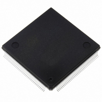
ST10F269Z2Q6/TR STMicroelectronics, ST10F269Z2Q6/TR Datasheet - Page 35

ST10F269Z2Q6/TR
Manufacturer Part Number
ST10F269Z2Q6/TR
Description
MCU 16BIT 256KBIT FLASH 144-PQFP
Manufacturer
STMicroelectronics
Series
ST10r
Datasheet
1.ST10F269Z2Q3.pdf
(184 pages)
Specifications of ST10F269Z2Q6/TR
Core Processor
ST10
Core Size
16-Bit
Speed
40MHz
Connectivity
CAN, EBI/EMI, SSC, UART/USART
Peripherals
POR, PWM, WDT
Number Of I /o
111
Program Memory Size
256KB (256K x 8)
Program Memory Type
FLASH
Ram Size
12K x 8
Voltage - Supply (vcc/vdd)
4.5 V ~ 5.5 V
Data Converters
A/D 16x10b
Oscillator Type
Internal
Operating Temperature
-40°C ~ 85°C
Package / Case
144-QFP
Processor Series
ST10F26x
Core
ST10
Data Bus Width
16 bit
Data Ram Size
12 KB
Interface Type
CAN, SSC, USART
Maximum Clock Frequency
40 MHz
Number Of Programmable I/os
111
Number Of Timers
5
Maximum Operating Temperature
+ 85 C
Mounting Style
SMD/SMT
Minimum Operating Temperature
- 40 C
On-chip Adc
10 bit, 16 Channel
Lead Free Status / RoHS Status
Lead free / RoHS Compliant
Eeprom Size
-
Lead Free Status / Rohs Status
Details
Available stocks
Company
Part Number
Manufacturer
Quantity
Price
Company:
Part Number:
ST10F269Z2Q6/TR
Manufacturer:
STMicroelectronics
Quantity:
10 000
- Current page: 35 of 184
- Download datasheet (4Mb)
ST10F269
6 - CENTRAL PROCESSING UNIT (CPU)
The CPU includes a 4-stage instruction pipeline, a
16-bit arithmetic and logic unit (ALU) and dedi-
cated SFRs. Additional hardware has been added
for a separate multiply and divide unit, a bit-mask
generator and a barrel shifter.
Most of the ST10F269 instructions can be exe-
cuted in one instruction cycle which requires 50ns
at 40MHz CPU clock (PQFP144 devices) and
62.5ns at 32MHz CPU clock (TQFP144 devices).
For example, shift and rotate instructions are pro-
cessed in one instruction cycle independent of the
number of bits to be shifted.
Multiple-cycle instructions have been optimized:
branches are carried out in 2 cycles, 16 x 16-bit
multiplication in 5 cycles and a 32/16-bit division
in 10 cycles.
The jump cache reduces the execution time of
repeatedly performed jumps in a loop, from
2 cycles to 1 cycle.
Figure 9 : CPU Block Diagram (MAC Unit not included)
128K/256K Byte
memory
Flash
32
Exec. Unit
BUSCON 0
BUSCON 1
BUSCON 2
BUSCON 3
BUSCON 4
Data Pg. Ptrs
Instr. Ptr
STKUN
SYSCON
STKOV
Pipeline
PSW
4-Stage
SP
ADDRSEL 1
ADDRSEL 2
ADDRSEL 3
ADDRSEL 4
Code Seg. Ptr.
Bit-Mask Gen.
Mul./Div.-HW
Barrel-Shift
CPU
16-Bit
MDH
MDL
ALU
CP
The CPU uses a bank of 16 word registers to run
the current context. This bank of General Purpose
Registers (GPR) is physically stored within the
on-chip Internal RAM (IRAM) area. A Context
Pointer (CP) register determines the base
address of the active register bank to be accessed
by the CPU.
The number of register banks is only restricted by
the available Internal RAM space. For easy
parameter passing, a register bank may overlap
others.
A system stack of up to 1024 bytes is provided as
a storage for temporary data. The system stack is
allocated in the on-chip RAM area, and it is
accessed by the CPU via the stack pointer (SP)
register.
Two separate SFRs, STKOV and STKUN, are
implicitly compared against the stack pointer
value upon each stack access for the detection of
a stack overflow or underflow.
6 - CENTRAL PROCESSING UNIT (CPU)
Registers
General
Purpose
R15
R0
16
16
2K Byte
Internal
Bank
Bank
Bank
RAM
n
0
i
35/184
Related parts for ST10F269Z2Q6/TR
Image
Part Number
Description
Manufacturer
Datasheet
Request
R

Part Number:
Description:
ST10F269-Q316-BIT MCU WITH MAC UNIT, 256K BYTE FLASH MEMORY AND 12K BYTE RAM
Manufacturer:
STMicroelectronics
Datasheet:

Part Number:
Description:
16Bit MCU 256K BYTE FLASH,12K BYTE RAM
Manufacturer:
STMicroelectronics
Datasheet:

Part Number:
Description:
MCU 16BIT 256K FLASH 144PQFP
Manufacturer:
STMicroelectronics
Datasheet:

Part Number:
Description:
Manufacturer:
STMicroelectronics
Datasheet:

Part Number:
Description:
MCU 16BIT 256K FLASH 144TQFP
Manufacturer:
STMicroelectronics

Part Number:
Description:
MCU 16BIT 256K FLASH 144PQFP
Manufacturer:
STMicroelectronics
Datasheet:

Part Number:
Description:
MCU 16BIT 256K FLASH 144PQFP
Manufacturer:
STMicroelectronics
Datasheet:

Part Number:
Description:
St10f269 16-bit Mcu With Mac Unit, 256k Byte Flash Memory And 12k Byte Ram
Manufacturer:
STMicroelectronics
Datasheet:

Part Number:
Description:
STMicroelectronics [RIPPLE-CARRY BINARY COUNTER/DIVIDERS]
Manufacturer:
STMicroelectronics
Datasheet:

Part Number:
Description:
STMicroelectronics [LIQUID-CRYSTAL DISPLAY DRIVERS]
Manufacturer:
STMicroelectronics
Datasheet:

Part Number:
Description:
BOARD EVAL FOR MEMS SENSORS
Manufacturer:
STMicroelectronics
Datasheet:


