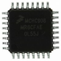
MCHC908MR8CFAE Freescale Semiconductor, MCHC908MR8CFAE Datasheet - Page 344

MCHC908MR8CFAE
Manufacturer Part Number
MCHC908MR8CFAE
Description
IC MCU 8K FLASH 8MHZ PWM 32-LQFP
Manufacturer
Freescale Semiconductor
Series
HC08r
Datasheet
1.MCHC908MR8VFAE.pdf
(372 pages)
Specifications of MCHC908MR8CFAE
Core Processor
HC08
Core Size
8-Bit
Speed
8MHz
Connectivity
SCI
Peripherals
LVD, POR, PWM
Number Of I /o
16
Program Memory Size
8KB (8K x 8)
Program Memory Type
FLASH
Ram Size
256 x 8
Voltage - Supply (vcc/vdd)
4.5 V ~ 5.5 V
Data Converters
A/D 7x10b
Oscillator Type
Internal
Operating Temperature
-40°C ~ 85°C
Package / Case
32-LQFP
Controller Family/series
HC08
No. Of I/o's
16
Ram Memory Size
256Byte
Cpu Speed
8MHz
No. Of Timers
2
Rohs Compliant
Yes
Processor Series
HC08MR
Core
HC08
Data Bus Width
8 bit
Data Ram Size
64 B
Interface Type
SCI, SPI
Maximum Clock Frequency
8 MHz
Number Of Programmable I/os
32
Number Of Timers
4
Operating Supply Voltage
0 V to 5 V
Maximum Operating Temperature
+ 85 C
Mounting Style
SMD/SMT
Development Tools By Supplier
FSICEBASE, M68CBL05CE
Minimum Operating Temperature
- 40 C
On-chip Adc
8 bit, 8 Channel
Lead Free Status / RoHS Status
Lead free / RoHS Compliant
Eeprom Size
-
Lead Free Status / Rohs Status
Details
Available stocks
Company
Part Number
Manufacturer
Quantity
Price
Company:
Part Number:
MCHC908MR8CFAE
Manufacturer:
Freescale Semiconductor
Quantity:
10 000
- Current page: 344 of 372
- Download datasheet (4Mb)
Electrical Specifications
Technical Data
344
Low-voltage inhibit falling
Low-voltage reset/recover hysteresis
Low-voltage recover rising
POR re-arm voltage
POR rise time ramp rate
1. V
2. Typical values reflect average measurements at midpoint of voltage range, 25°C only.
3. Run (operating) I
4. Wait I
5. Quiescent I
6. Maximum is highest guaranteed voltage for POR.
7. Maximum is the highest possible voltage for POR. If minimum V
loads; less than 100 pF on all outputs; C
affects run I
than 100 pF on all outputs; C
measured with PLL and LVI enabled
through combination of V
RST must be driven low externally until minimum V
DD
= 5.0 Vdc ±10%, V
DD
measured using external square wave clock source (f
DD
DD
; measured with all modules enabled
measured with PLL and LVI disengaged; OCS1 grounded; no port pins sourcing current. It is measured
DD
Characteristic
(6)
measured using external square wave clock source (f
SS
(7)
DD
= 0 Vdc, T
and V
L
= 20 pF on OSC2; all ports configured as inputs; OSC2 capacitance linearly affects wait I
(1)
DDA
A
.
= T
L
L
= 20 pF on OSC2; all ports configured as inputs; OSC2 capacitance linearly
to T
Electrical Specifications
H
, unless otherwise noted
DD
is reached.
Symbol
V
V
V
V
R
LVRR2
OSC
DD
LVRF2
LVH2
POR
POR
is not reached before the internal POR reset is released,
= 8.2 MHz); all inputs 0.2 V from rail; no dc loads; less
OSC
0.035
Min
3.8
= 8.2 MHz); all inputs 0.2 V from rail; no dc
50
—
0
Typ
MC68HC908MR8 — Rev 4.1
100
4.1
4.2
—
—
Freescale Semiconductor
(2)
Max
100
4.6
—
—
—
— Continued
V/ms
Unit
mV
mV
V
V
DD
;
Related parts for MCHC908MR8CFAE
Image
Part Number
Description
Manufacturer
Datasheet
Request
R
Part Number:
Description:
Manufacturer:
Freescale Semiconductor, Inc
Datasheet:
Part Number:
Description:
Manufacturer:
Freescale Semiconductor, Inc
Datasheet:
Part Number:
Description:
Manufacturer:
Freescale Semiconductor, Inc
Datasheet:
Part Number:
Description:
Manufacturer:
Freescale Semiconductor, Inc
Datasheet:
Part Number:
Description:
Manufacturer:
Freescale Semiconductor, Inc
Datasheet:
Part Number:
Description:
Manufacturer:
Freescale Semiconductor, Inc
Datasheet:
Part Number:
Description:
Manufacturer:
Freescale Semiconductor, Inc
Datasheet:
Part Number:
Description:
Manufacturer:
Freescale Semiconductor, Inc
Datasheet:
Part Number:
Description:
Manufacturer:
Freescale Semiconductor, Inc
Datasheet:
Part Number:
Description:
Manufacturer:
Freescale Semiconductor, Inc
Datasheet:
Part Number:
Description:
Manufacturer:
Freescale Semiconductor, Inc
Datasheet:
Part Number:
Description:
Manufacturer:
Freescale Semiconductor, Inc
Datasheet:
Part Number:
Description:
Manufacturer:
Freescale Semiconductor, Inc
Datasheet:
Part Number:
Description:
Manufacturer:
Freescale Semiconductor, Inc
Datasheet:
Part Number:
Description:
Manufacturer:
Freescale Semiconductor, Inc
Datasheet:


