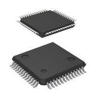
R5F21356CNFP#U0 Renesas Electronics America, R5F21356CNFP#U0 Datasheet - Page 679

R5F21356CNFP#U0
Manufacturer Part Number
R5F21356CNFP#U0
Description
MCU 1KB FLASH 32K ROM 52-LQFP
Manufacturer
Renesas Electronics America
Series
R8C/3x/35Cr
Datasheet
1.R5F21356CNFPU0.pdf
(762 pages)
Specifications of R5F21356CNFP#U0
Core Processor
R8C
Core Size
16/32-Bit
Speed
20MHz
Connectivity
I²C, LIN, SIO, SSU, UART/USART
Peripherals
POR, PWM, Voltage Detect, WDT
Number Of I /o
47
Program Memory Size
32KB (32K x 8)
Program Memory Type
FLASH
Ram Size
2.5K x 8
Voltage - Supply (vcc/vdd)
1.8 V ~ 5.5 V
Data Converters
A/D 12x10b; D/A 2x8b
Oscillator Type
Internal
Operating Temperature
-20°C ~ 85°C
Package / Case
52-LQFP
Lead Free Status / RoHS Status
Lead free / RoHS Compliant
Eeprom Size
-
Available stocks
Company
Part Number
Manufacturer
Quantity
Price
- Current page: 679 of 762
- Download datasheet (8Mb)
R8C/35C Group
REJ09B0567-0100 Rev.1.00 Dec. 14, 2009
Page 646 of 725
Figure 31.14
31.4.11.5 Lock Bit Program Command
This command is used to set the lock bit of any block in the program ROM area to 0 (locked).
When 77h is written in the first bus cycle and D0h is written in the second bus cycle to the starting block
address, 0 is written to the lock bit of the specified block. Make sure the address value in the first bus cycle is
the same address as the starting block address specified in the second bus cycle.
Figure 31.14 shows a Lock Bit Program Flowchart. The lock bit status (lock bit data) can be read using the read
lock bit status command.
The FST7 bit in the FST register can be used to confirm whether writing to the lock bit has completed.
Refer to 31.4.10 Data Protect Function for the lock bit function and how to set the lock bit to 1 (not locked).
Lock Bit Program Flowchart
Write the command code 77h
Write D0h to the starting
block address
Full status check
Completed
FST7 = 1?
Start
Yes
No
FST7: Bit in FST register
31. Flash Memory
Related parts for R5F21356CNFP#U0
Image
Part Number
Description
Manufacturer
Datasheet
Request
R

Part Number:
Description:
KIT STARTER FOR M16C/29
Manufacturer:
Renesas Electronics America
Datasheet:

Part Number:
Description:
KIT STARTER FOR R8C/2D
Manufacturer:
Renesas Electronics America
Datasheet:

Part Number:
Description:
R0K33062P STARTER KIT
Manufacturer:
Renesas Electronics America
Datasheet:

Part Number:
Description:
KIT STARTER FOR R8C/23 E8A
Manufacturer:
Renesas Electronics America
Datasheet:

Part Number:
Description:
KIT STARTER FOR R8C/25
Manufacturer:
Renesas Electronics America
Datasheet:

Part Number:
Description:
KIT STARTER H8S2456 SHARPE DSPLY
Manufacturer:
Renesas Electronics America
Datasheet:

Part Number:
Description:
KIT STARTER FOR R8C38C
Manufacturer:
Renesas Electronics America
Datasheet:

Part Number:
Description:
KIT STARTER FOR R8C35C
Manufacturer:
Renesas Electronics America
Datasheet:

Part Number:
Description:
KIT STARTER FOR R8CL3AC+LCD APPS
Manufacturer:
Renesas Electronics America
Datasheet:

Part Number:
Description:
KIT STARTER FOR RX610
Manufacturer:
Renesas Electronics America
Datasheet:

Part Number:
Description:
KIT STARTER FOR R32C/118
Manufacturer:
Renesas Electronics America
Datasheet:

Part Number:
Description:
KIT DEV RSK-R8C/26-29
Manufacturer:
Renesas Electronics America
Datasheet:

Part Number:
Description:
KIT STARTER FOR SH7124
Manufacturer:
Renesas Electronics America
Datasheet:

Part Number:
Description:
KIT STARTER FOR H8SX/1622
Manufacturer:
Renesas Electronics America
Datasheet:

Part Number:
Description:
KIT DEV FOR SH7203
Manufacturer:
Renesas Electronics America
Datasheet:


