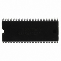
M38588GCSP#U0 Renesas Electronics America, M38588GCSP#U0 Datasheet - Page 24

M38588GCSP#U0
Manufacturer Part Number
M38588GCSP#U0
Description
IC 740/3858 MCU QZ-ROM 42DIP
Manufacturer
Renesas Electronics America
Series
740/38000r
Datasheet
1.M38588GCFPU0.pdf
(77 pages)
Specifications of M38588GCSP#U0
Core Processor
740
Core Size
8-Bit
Speed
12.5MHz
Connectivity
SIO, UART/USART
Peripherals
PWM, WDT
Number Of I /o
34
Program Memory Size
48KB (48K x 8)
Program Memory Type
QzROM
Ram Size
1.5K x 8
Voltage - Supply (vcc/vdd)
2.7 V ~ 5.5 V
Data Converters
A/D 9x8b
Oscillator Type
Internal
Operating Temperature
-20°C ~ 85°C
Package / Case
42-DIP (0.600", 15.24mm)
Lead Free Status / RoHS Status
Lead free / RoHS Compliant
Eeprom Size
-
Available stocks
Company
Part Number
Manufacturer
Quantity
Price
3858 Group
TIMERS
The 3858 group has four 8-bit timers: timer 1, timer 2, timer X, and
timer Y.
The timer 1 and timer 2 use one prescaler in common, and the
timer X and timer Y use each prescaler. Those are 8-bit
prescalers. Each of the timers and prescalers has a timer latch or
a prescaler latch.
The division ratio of each timer or prescaler is given by 1/(n + 1),
where n is the value in the corresponding timer or prescaler latch.
All timers are down-counters. When the timer reaches “00
underflow occurs at the next count pulse and the contents of the
corresponding timer latch are reloaded into the timer and the
count is continued. When the timer underflows, the interrupt re-
quest bit corresponding to that timer is set to “1”.
The divider count source is switched by the main clock division
ratio selection bits of CPU mode register (bits 7 and 6 at address
003B
(middle-speed mode), X
(low-speed mode), X
The prescaler 12 counts the output of the timer divider. The count
source is selected by the timer 12, X count source selection
register (address 002E
128, 1/256, 1/512, 1/1024 of f(X
Timer 1 and Timer 2
The timer 1 and timer 2 counts the output of prescaler 12 and pe-
riodically set the interrupt request bit.
The prescaler X and prescaler Y count the output of the timer
divider or f(X
count source selection register (address 002E
Z1 count source selection register (address 002F
1/4, 1/8, 1/16, 1/32, 1/64, 1/128, 1/256, 1/512, and 1/1024 of f(X
or f(X
REJ03B0139-0111
page 22 of 73
Timer divider
Prescaler 12
Prescaler X and prescaler Y
8-bit Timers
16
CIN
). When these bits are “00” (high-speed mode) or “01”
); and f(X
CIN
). The count source is selected by the timer 12, X
CIN
CIN
).
16
Rev.1.11
is selected.
IN
) among 1/2, 1/4, 1/8, 1/16, 1/32, 1/64, 1/
is selected. When these bits are “10”
IN
) or f(X
Dec 18, 2008
CIN
).
16
) and the timer Y,
16
) among 1/2,
16
”, an
IN
)
Timer X and Timer Y
The timer X and timer Y can each select one of four operating
modes by setting the timer XY mode register (address 0023
(1) Timer mode
This mode can be selected by setting “00” to the timer X operating
mode bits (bits 1 and 0) and the timer Y operating mode bits (bits
5 and 4) of the timer XY mode register (address 0023
The timer count operation is started by setting “0” to the timer X
count stop bit (bit 3) and the timer Y count stop bit (bit 7) of the
timer XY mode register (address 0023
When the timer reaches “00
count pulse and the contents of timer latch are reloaded into the
timer and the count is continued.
(2) Pulse output mode
This mode can be selected by setting “01” to the timer X operating
mode bits (bits 1 and 0) and the timer Y operating mode bits (bits
5 and 4) of the timer XY mode register (address 0023
The operation is the same as the timer mode’s. Moreover the
pulse which is inverted each time the timer underflows is output
from CNTR
the output of CNTR
fied by their active edge switch bits when writing to the timer.
When the CNTR
tive edge switch bit (bit 6) of the timer XY mode register (address
0023
output starts with “L” level.
Switching the CNTR
the output level of the corresponding CNTR
Set the double-function port of CNTR
P4
Precautions
Mode selection
Explanation of operation
Mode selection
Explanation of operation
0
to output in this mode.
16
) is “0”, the output starts with “H” level. When it is “1”, the
0
/CNTR
0
active edge switch bit (bit 2) and the CNTR
1
0
0
/CNTR
pin. Regardless of the timer counting or not
or CNTR
1
16
pin is initialized to the level of speci-
1
”, an underflow occurs at the next
active edge switch bit will reverse
16
0
/CNTR
).
0
or CNTR1 pin.
1
pin and port P2
16
16
).
).
16
1
).
ac-
7
/


