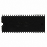
M38588GCSP#U0 Renesas Electronics America, M38588GCSP#U0 Datasheet - Page 47

M38588GCSP#U0
Manufacturer Part Number
M38588GCSP#U0
Description
IC 740/3858 MCU QZ-ROM 42DIP
Manufacturer
Renesas Electronics America
Series
740/38000r
Datasheet
1.M38588GCFPU0.pdf
(77 pages)
Specifications of M38588GCSP#U0
Core Processor
740
Core Size
8-Bit
Speed
12.5MHz
Connectivity
SIO, UART/USART
Peripherals
PWM, WDT
Number Of I /o
34
Program Memory Size
48KB (48K x 8)
Program Memory Type
QzROM
Ram Size
1.5K x 8
Voltage - Supply (vcc/vdd)
2.7 V ~ 5.5 V
Data Converters
A/D 9x8b
Oscillator Type
Internal
Operating Temperature
-20°C ~ 85°C
Package / Case
42-DIP (0.600", 15.24mm)
Lead Free Status / RoHS Status
Lead free / RoHS Compliant
Eeprom Size
-
Available stocks
Company
Part Number
Manufacturer
Quantity
Price
3858 Group
Fig. 39 Operation of UART serial I/O1 function
[Transmit Buffer Register/Receive Buffer
Register (TB/RB)] 0018
The transmit buffer register and the receive buffer register are lo-
cated at the same address. The transmit buffer is write-only and
the receive buffer is read-only. If a character bit length is 7 bits, the
MSB of data stored in the receive buffer is “0”.
[Serial I/O1 Status Register (SIOSTS)] 0019
The read-only serial I/O1 status register consists of seven flags
(bits 0 to 6) which indicate the operating status of the serial I/O1
function and various errors.
Three of the flags (bits 4 to 6) are valid only in UART mode.
The receive buffer full flag (bit 1) is cleared to “0” when the receive
buffer register is read.
If there is an error, it is detected at the same time that data is
transferred from the receive shift register to the receive buffer reg-
ister, and the receive buffer full flag is set. A write to the serial I/O1
status register clears all the error flags OE, PE, FE, and SE (bit 3
to bit 6, respectively). Writing “0” to the serial I/O1 enable bit SIOE
(bit 7 of the serial I/O1 control register) also clears all the status
flags, including the error flags.
Bits 0 to 6 of the serial I/O1 status register are initialized to “0” at
reset, but if the transmit enable bit (bit 4) of the serial I/O1 control
register has been set to “1”, the transmit shift completion flag (bit
2) and the transmit buffer empty flag (bit 0) become “1”.
REJ03B0139-0111
page 45 of 73
Transmit or receive clock
Transmit buffer write
Receive buffer read
Serial output T
Notes
Serial input R
1: Error flag detection occurs at the same time that the RBF flag becomes “1” (at 1st stop bit, during reception).
2: As the transmit interrupt (TI), when either the TBE or TSC flag becomes “1”, can be selected to occur depending on the setting of the transmit
3: The receive interrupt (RI) is set when the RBF flag becomes “1”.
4: After data is written to the transmit buffer when TSC=1, 0.5 to 1.5 cycles of the data shift cycle is necessary until changing to TSC=0.
signal
signal
interrupt source selection bit (TIC) of the serial I/O1 control register.
X
X
D
D
Rev.1.11
TBE=0
TSC=0
TBE=1
16
ST
ST
Dec 18, 2008
D
D
0
0
TBE=0
D
D
1
1
1 start bit
7 or 8 data bit
1 or 0 parity bit
1 or 2 stop bit (s)
16
[Serial I/O1 Control Register (SIOCON)] 001A
The serial I/O1 control register consists of eight control bits for the
serial I/O1 function.
[UART Control Register (UARTCON)] 001B
The UART control register consists of four control bits (bits 0 to 3)
which are valid when asynchronous serial I/O is selected and set
the data format of an data transfer and one bit (bit 4) which is al-
ways valid and sets the output structure of the P2
[Baud Rate Generator (BRG)] 001C
The baud rate generator determines the baud rate for serial trans-
fer.
The baud rate generator divides the frequency of the count source
by 1/(n + 1), where n is the value written to the baud rate genera-
tor.
RBF=1
SP
SP
TBE=1
ST
ST
D
0
D
0
RBF=0
D
D
1
1
Generated at 2nd bit in 2-stop-bit mode
5
/T
16
X
D pin.
SP
TSC=1
RBF=1
SP
16
16


