MC908GT16CBE Freescale Semiconductor, MC908GT16CBE Datasheet - Page 22
MC908GT16CBE
Manufacturer Part Number
MC908GT16CBE
Description
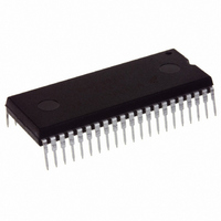
IC MCU 16K FLASH 8MHZ SPI 42SDIP
Manufacturer
Freescale Semiconductor
Series
HC08r
Datasheet
1.MC908GT8CFBE.pdf
(292 pages)
Specifications of MC908GT16CBE
Core Processor
HC08
Core Size
8-Bit
Speed
8MHz
Connectivity
SCI, SPI
Peripherals
LVD, POR, PWM
Number Of I /o
36
Program Memory Size
16KB (16K x 8)
Program Memory Type
FLASH
Ram Size
512 x 8
Voltage - Supply (vcc/vdd)
2.7 V ~ 5.5 V
Data Converters
A/D 8x8b
Oscillator Type
Internal
Operating Temperature
-40°C ~ 85°C
Package / Case
42-DIP (0.600", 15.24mm)
Controller Family/series
HC08
No. Of I/o's
34
Ram Memory Size
512Byte
Cpu Speed
8MHz
No. Of Timers
2
Embedded Interface Type
I2C, SCI, SPI
Rohs Compliant
Yes
Processor Series
HC08GT
Core
HC08
Data Bus Width
8 bit
Data Ram Size
512 B
Interface Type
SCI, SPI
Maximum Clock Frequency
8 MHz
Number Of Programmable I/os
30
Number Of Timers
4
Operating Supply Voltage
0 V to 5 V
Maximum Operating Temperature
+ 85 C
Mounting Style
Through Hole
Development Tools By Supplier
FSICEBASE, DEMO908GZ60E, M68CBL05CE, M68EML08GPGTE
Minimum Operating Temperature
- 40 C
On-chip Adc
8 bit, 8 Channel
Package
42SPDIP
Family Name
HC08
Maximum Speed
8 MHz
Lead Free Status / RoHS Status
Lead free / RoHS Compliant
Eeprom Size
-
Lead Free Status / Rohs Status
Details


General Description
22
•
•
•
•
•
•
•
•
•
•
•
•
•
•
•
•
•
•
•
•
•
•
•
System protection features:
–
–
–
–
Low-power design; fully static with stop and wait modes
Standard low-power modes of operation:
–
–
Master reset pin and power-on reset (POR)
16 Kbytes of on-chip 100k cycle write/erase capable Flash memory (8 Kbytes on
MC68HC908GT8)
512 bytes of on-chip random-access memory (RAM)
720 bytes of Flash programming routines ROM
Serial peripheral interface module (SPI)
Serial communications interface module (SCI)
Two 16-bit, 2-channel timer interface modules (TIM1 and TIM2) with selectable input capture,
output compare, and pulse-width modulation (PWM) capability on each channel
8-channel, 8-bit successive approximation analog-to-digital converter (ADC)
Break module (BRK) to allow single breakpoint setting during in-circuit debugging
Internal pullups on IRQ and RST to reduce customer system cost
Up to 36 general-purpose input/output (I/O) pins, including:
–
–
Selectable pullups on inputs only on ports A, C, and D. Selection is on an individual port bit basis.
During output mode, pullups are disengaged.
High current 10-mA sink/10-mA source capability on all port pins
Higher current 20-mA sink/source capability on PTC0–PTC4
Timebase module with clock prescaler circuitry for eight user selectable periodic real-time
interrupts with optional active clock source during stop mode for periodic wakeup from stop using
an external 32-kHz crystal or internal oscillator
User selection of having the oscillator enabled or disabled during stop mode
8-bit keyboard wakeup port
Available packages:
–
–
Specific features of the MC68HC908GT16 in 42-pin SDIP are:
–
–
Specific features of the MC68HC908GT16 in 44-pin QFP are:
–
–
Optional computer operating properly (COP) reset
Low-voltage detection with optional reset and selectable trip points for 3.0-V and 5.0-V
operation
Illegal opcode detection with reset
Illegal address detection with reset
Wait mode
Stop mode
28 shared-function I/O pins
Six or eight dedicated I/O pins, depending on package choice
42-pin shrink dual in-line package (SDIP)
44-pin quad flat pack (QFP)
Port C is only 5 bits: PTC0–PTC4
Port D is 8 bits: PTD0–PTD7; dual 2-channel TIM modules
Port C is 7 bits: PTC0–PTC6
Port D is 8 bits: PTD0–PTD7; dual 2-channel TIM modules
MC68HC908GT16 • MC68HC908GT8 • MC68HC08GT16 Data Sheet, Rev. 5.0
Freescale Semiconductor
Related parts for MC908GT16CBE
Image
Part Number
Description
Manufacturer
Datasheet
Request
R

Part Number:
Description:
Manufacturer:
Freescale Semiconductor, Inc
Datasheet:
Part Number:
Description:
Manufacturer:
Freescale Semiconductor, Inc
Datasheet:
Part Number:
Description:
Manufacturer:
Freescale Semiconductor, Inc
Datasheet:
Part Number:
Description:
Manufacturer:
Freescale Semiconductor, Inc
Datasheet:
Part Number:
Description:
Manufacturer:
Freescale Semiconductor, Inc
Datasheet:
Part Number:
Description:
Manufacturer:
Freescale Semiconductor, Inc
Datasheet:
Part Number:
Description:
Manufacturer:
Freescale Semiconductor, Inc
Datasheet:
Part Number:
Description:
Manufacturer:
Freescale Semiconductor, Inc
Datasheet:
Part Number:
Description:
Manufacturer:
Freescale Semiconductor, Inc
Datasheet:
Part Number:
Description:
Manufacturer:
Freescale Semiconductor, Inc
Datasheet:
Part Number:
Description:
Manufacturer:
Freescale Semiconductor, Inc
Datasheet:
Part Number:
Description:
Manufacturer:
Freescale Semiconductor, Inc
Datasheet:
Part Number:
Description:
Manufacturer:
Freescale Semiconductor, Inc
Datasheet:
Part Number:
Description:
Manufacturer:
Freescale Semiconductor, Inc
Datasheet:
Part Number:
Description:
Manufacturer:
Freescale Semiconductor, Inc
Datasheet: