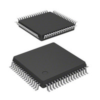
M30281F8HP#D5 Renesas Electronics America, M30281F8HP#D5 Datasheet - Page 113

M30281F8HP#D5
Manufacturer Part Number
M30281F8HP#D5
Description
IC M16C MCU FLASH 64K 64-LQFP
Manufacturer
Renesas Electronics America
Series
M16C™ M16C/Tiny/28r
Datasheet
1.M30280F6HPU9.pdf
(425 pages)
Specifications of M30281F8HP#D5
Core Processor
M16C/60
Core Size
16-Bit
Speed
20MHz
Connectivity
I²C, IEBus, SIO, UART/USART
Peripherals
DMA, POR, PWM, Voltage Detect, WDT
Number Of I /o
55
Program Memory Size
64KB (64K x 8)
Program Memory Type
FLASH
Ram Size
4K x 8
Voltage - Supply (vcc/vdd)
2.7 V ~ 5.5 V
Data Converters
A/D 13x10b
Oscillator Type
Internal
Operating Temperature
-20°C ~ 85°C
Package / Case
64-LQFP
For Use With
M30290T2-CPE - EMULATOR COMPACT M16C/26A/28/29M30290T2-CPE-HP - EMULATOR COMPACT FOR M16C/TINY
Lead Free Status / RoHS Status
Contains lead / RoHS non-compliant
Eeprom Size
-
Available stocks
Company
Part Number
Manufacturer
Quantity
Price
Part Number:
M30281F8HP#D5M30281F8HP#U3
Manufacturer:
Renesas Electronics America
Quantity:
10 000
- Current page: 113 of 425
- Download datasheet (4Mb)
R
R
M
e
E
1
. v
Figure 11.3 DM1SL Register, DM0CON Register, and DM1CON Registers
J
6
0
C
2
9
0 .
2 /
B
0
0
8
0
4
G
J
7
a
o r
0 -
. n
NOTES:
NOTES:
DMA1 Request Cause Select Register
DMAi Control Register
b7
b7
u
DSEL3 to DSEL0
0 0 0 0
0 0 0 1
0 0 1 0
0 0 1 1
0 1 0 0
0 1 0 1
0 1 1 0
0 1 1 1
1 0 0 0
1 0 0 1
1 0 1 0
1 0 1 1
1 1 0 0
1 1 0 1
1 1 1 0
1 1 1 1
2
3
1. The causes of DMA1 requests can be selected by a combination of DMS bit and DSEL3 to DSEL0 bits in the
1. The DMAS bit can be set to “0” by writing “0” in a program (This bit remains unchanged even if “1” is written).
2. At least one of the DAD and DSD bits must be “0” (address direction fixed).
p
0
, 1
b6
b6
0
manner described below.
(
M
2
2
2
2
2
2
2
2
2
2
2
2
2
2
2
2
2
b5
b5
0
1
0
6
b4
b4
7
C
2 /
b3
b3
, 8
page 91
b2
b2
DMS=0(basic cause of request)
Falling edge of INT1 pin
Software trigger
Timer A0
Timer A1
Timer A2
Timer A3
Timer A4
Timer B0
Timer B1
Timer B2
UART0 transmit
UART0 receive
UART2 transmit
UART2 receive/ACK2
A/D conversion
UART1 receive
M
b1
b1
1
6
b0
b0
C
(i=0,1)
f o
2 /
Bit Symbol
Bit Symbol
8
(b7-b6)
DMBIT
DMASL
DMAS
DMAE
3
DSEL0
DSEL1
DSEL2
DSEL3
(b5-b4)
DMS
DSR
DSD
DAD
) B
8
Symbol
DM1SL
Symbol
DM0CON
DM1CON
5
Transfer unit bit select bit
Repeat transfer mode
select bit
DMA request bit
DMA enable bit
Source address direction
select bit
Destination address
direction select bit
DMA request cause
select bit
Nothing is assigned. When write, set to “0”.
When read, its content is “0”.
DMA request cause
expansion select bit
Software DMA
request bit
Nothing is assigned. When write, set to “0”. When
read, its content is “0”.
Bit Name
Bit Name
(2)
DMS=1(extended cause of request)
IC/OC base timer
–
IC/OC channel 0
IC/OC channel 1
–
SI/O3
SI/O4
Two edges of INT1
–
–
IC/OC channel 2
IC/OC channel 3
IC/OC channel 4
IC/OC channel 5
IC/OC channel 6
IC/OC channel 7
Address
002C
003C
03BA
Address
(2)
16
16
16
Refer to note (1)
A DMA request is generated by
setting this bit to “1” when the DMS
bit is “0” (basic cause) and the
DSEL3 to DSEL0 bits are “0001
(software trigger).
The value of this bit when read is “0” .
0: Basic cause of request
1: Extended cause of request
0 : 16 bits
1 : 8 bits
0 : Single transfer
1 : Repeat transfer
0 : DMA not requested
1 : DMA requested
0 : Disabled
1 : Enabled
0 : Fixed
1 : Forward
0 : Fixed
1 : Forward
After Reset
00000X00
00000X00
Function
After Reset
00
Function
16
2
2
2
”
RW
RW
RW
RW
RW
RW
RW
RW
RW
RW
RW
RW
RW
RW
(1)
11. DMAC
Related parts for M30281F8HP#D5
Image
Part Number
Description
Manufacturer
Datasheet
Request
R

Part Number:
Description:
KIT STARTER FOR M16C/29
Manufacturer:
Renesas Electronics America
Datasheet:

Part Number:
Description:
KIT STARTER FOR R8C/2D
Manufacturer:
Renesas Electronics America
Datasheet:

Part Number:
Description:
R0K33062P STARTER KIT
Manufacturer:
Renesas Electronics America
Datasheet:

Part Number:
Description:
KIT STARTER FOR R8C/23 E8A
Manufacturer:
Renesas Electronics America
Datasheet:

Part Number:
Description:
KIT STARTER FOR R8C/25
Manufacturer:
Renesas Electronics America
Datasheet:

Part Number:
Description:
KIT STARTER H8S2456 SHARPE DSPLY
Manufacturer:
Renesas Electronics America
Datasheet:

Part Number:
Description:
KIT STARTER FOR R8C38C
Manufacturer:
Renesas Electronics America
Datasheet:

Part Number:
Description:
KIT STARTER FOR R8C35C
Manufacturer:
Renesas Electronics America
Datasheet:

Part Number:
Description:
KIT STARTER FOR R8CL3AC+LCD APPS
Manufacturer:
Renesas Electronics America
Datasheet:

Part Number:
Description:
KIT STARTER FOR RX610
Manufacturer:
Renesas Electronics America
Datasheet:

Part Number:
Description:
KIT STARTER FOR R32C/118
Manufacturer:
Renesas Electronics America
Datasheet:

Part Number:
Description:
KIT DEV RSK-R8C/26-29
Manufacturer:
Renesas Electronics America
Datasheet:

Part Number:
Description:
KIT STARTER FOR SH7124
Manufacturer:
Renesas Electronics America
Datasheet:

Part Number:
Description:
KIT STARTER FOR H8SX/1622
Manufacturer:
Renesas Electronics America
Datasheet:

Part Number:
Description:
KIT DEV FOR SH7203
Manufacturer:
Renesas Electronics America
Datasheet:


