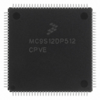
MC9S12DP512CPVER Freescale Semiconductor, MC9S12DP512CPVER Datasheet - Page 17

MC9S12DP512CPVER
Manufacturer Part Number
MC9S12DP512CPVER
Description
IC MCU 16BIT 4K FLASH 112-LQFP
Manufacturer
Freescale Semiconductor
Series
HCS12r
Datasheet
1.MC9S12DP512CPVE.pdf
(124 pages)
Specifications of MC9S12DP512CPVER
Core Processor
HCS12
Core Size
16-Bit
Speed
25MHz
Connectivity
CAN, I²C, SCI, SPI
Peripherals
PWM, WDT
Number Of I /o
91
Program Memory Size
512KB (512K x 8)
Program Memory Type
FLASH
Eeprom Size
4K x 8
Ram Size
12K x 8
Voltage - Supply (vcc/vdd)
2.35 V ~ 5.25 V
Data Converters
A/D 16x10b
Oscillator Type
Internal
Operating Temperature
-40°C ~ 85°C
Package / Case
112-LQFP
Package
112LQFP
Family Name
HCS12
Maximum Speed
25 MHz
Operating Supply Voltage
2.5|5 V
Data Bus Width
16 Bit
Interface Type
CAN/I2C/SCI/SPI
On-chip Adc
2(8-chx10-bit)
Number Of Timers
8
Lead Free Status / RoHS Status
Lead free / RoHS Compliant
Other names
MC9S12DP512CPVERTR
Available stocks
Company
Part Number
Manufacturer
Quantity
Price
Company:
Part Number:
MC9S12DP512CPVER
Manufacturer:
Freescale Semiconductor
Quantity:
10 000
Document References
The Device Guide provides information about the MC9S12DP512 device made up of standard HCS12
blocks and the HCS12 processor core.
This document is part of the customer documentation. A complete set of device manuals also includes the
individual Block Guides of the implemented modules. In an effort to reduce redundancy, all module
specific information is located only in the respective Block Guide. If applicable, special implementation
details of the module are given in the block description sections of this document.
See Table 0-2 for names and versions of the referenced documents throughout the Device Guide.
Analog to Digital Converter 10 Bit 8 Channel (ATD_10B8C) Block Guide
Enhanced Capture Timer 16 Bit 8 Channel (ECT_16B8C) Block Guide
Pulse Width Modulator 8 Bit 8 Channel (PWM_8B8C) Block Guide
– The CAN4 pin functionality (TXCAN4, RXCAN4) is not available on port PJ7, PJ6, PM7,
– The BDLC pin functionality (TXB, RXB) is not available on port PM1 and PM0, if using a
– Do not write MODRR1 and MODRR0 bits of Module Routing Register (PIM_9DP256 Block
– Do not write MODRR3 and MODRR2 bits of Module Routing Register (PIM_9DP256 Block
HCS12 Multiplexed External Bus Interface (MEBI) Block Guide
PM6, PM5 and PM4, if using a derivative without CAN0.
derivative without BDLC.
Guide), if using a derivative without CAN0.
Guide), if using a derivative without CAN4.
Byte Level Data Link Controller -J1850 (BDLC) Block Guide
HCS12 Module Mapping Control (MMC) Block Guide
Port Integration Module (PIM_9DP256) Block Guide
Asynchronous Serial Interface (SCI) Block Guide
Clock and Reset Generator (CRG) Block Guide
HCS12 Background Debug (BDM) Block Guide
Freescale Scalable CAN (MSCAN) Block Guide
Serial Peripheral Interface (SPI) Block Guide
Block Guide
512K Byte Flash (FTS512K4) Block Guide
4K Byte EEPROM (EETS4K) Block Guide
Voltage Regulator (VREG) Block Guide
HCS12 Breakpoint (BKP) Block Guide
HCS12 Interrupt (INT) Block Guide
Table 0-2 Document References
HCS12 CPU Reference Manual
Inter IC Bus (IIC) Block Guide
Oscillator (OSC) Block Guide
1
Version
V02
V04
V03
V01
V04
V01
V04
V01
V02
V02
V02
V03
V01
V01
V02
V01
V01
V03
V02
V02
MC9S12DP512 Device Guide V01.25
Document Order Number
S12ATD10B8CV2/D
S12PWM8B8CV1/D
S12FTS512K4V1/D
S12DP256PIMV3/D
S12ECT16B8V1/D
S12EETS4KV2/D
S12VREGV1/D
S12BDLCV1/D
S12MEBIV3/D
S12MMCV4/D
S12MSCANV2/D
S12BDMV4/D
S12CRGV4/D
S12OSCV2/D
S12CPUV2/D
S12BKPV1/D
S12SCIV2/D
S12INTV1/D
S12SPIV3/D
S12IICV2/D
17


