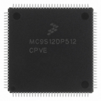
MC9S12DP512CPVER Freescale Semiconductor, MC9S12DP512CPVER Datasheet - Page 89

MC9S12DP512CPVER
Manufacturer Part Number
MC9S12DP512CPVER
Description
IC MCU 16BIT 4K FLASH 112-LQFP
Manufacturer
Freescale Semiconductor
Series
HCS12r
Datasheet
1.MC9S12DP512CPVE.pdf
(124 pages)
Specifications of MC9S12DP512CPVER
Core Processor
HCS12
Core Size
16-Bit
Speed
25MHz
Connectivity
CAN, I²C, SCI, SPI
Peripherals
PWM, WDT
Number Of I /o
91
Program Memory Size
512KB (512K x 8)
Program Memory Type
FLASH
Eeprom Size
4K x 8
Ram Size
12K x 8
Voltage - Supply (vcc/vdd)
2.35 V ~ 5.25 V
Data Converters
A/D 16x10b
Oscillator Type
Internal
Operating Temperature
-40°C ~ 85°C
Package / Case
112-LQFP
Package
112LQFP
Family Name
HCS12
Maximum Speed
25 MHz
Operating Supply Voltage
2.5|5 V
Data Bus Width
16 Bit
Interface Type
CAN/I2C/SCI/SPI
On-chip Adc
2(8-chx10-bit)
Number Of Timers
8
Lead Free Status / RoHS Status
Lead free / RoHS Compliant
Other names
MC9S12DP512CPVERTR
Available stocks
Company
Part Number
Manufacturer
Quantity
Price
Company:
Part Number:
MC9S12DP512CPVER
Manufacturer:
Freescale Semiconductor
Quantity:
10 000
A.1.7 Operating Conditions
This chapter describes the operating conditions of the device. Unless otherwise noted those conditions
apply to all the following data.
A.1.8 Power Dissipation and Thermal Characteristics
Power dissipation and thermal characteristics are closely related. The user must assure that the maximum
operating junction temperature is not exceeded. The average chip-junction temperature (T
obtained from:
NOTE:
I/O, Regulator and Analog Supply Voltage
Digital Logic Supply Voltage
PLL Supply Voltage
Voltage Difference VDDX to VDDR and VDDA
Voltage Difference VSSX to VSSR and VSSA
Bus Frequency (MC9S12DP512C, V, M)
MC9S12DP512C
MC9S12DP512V
MC9S12DP512M
NOTES:
1. The device contains an internal voltage regulator to generate the logic and PLL supply out of the I/O supply. The
2. Some blocks e.g. ATD (conversion) and NVMs (program/erase) require higher bus frequencies for proper oper-
3. Please refer to Section A.1.8 Power Dissipation and Thermal Characteristics for more details about the rela-
given operating range applies when this regulator is disabled and the device is powered from an external source.
ation.
tion between ambient temperature T
Operating Ambient Temperature Range
Operating Ambient Temperature Range
Operating Ambient Temperature Range
Please refer to the temperature rating of the device (C, V, M) with regards to the
ambient temperature T
calculations refer to Section A.1.8 Power Dissipation and Thermal
Characteristics.
Operating Junction Temperature Range
Operating Junction Temperature Range
Operating Junction Temperature Range
(1)
Rating
1
Table A-4 Operating Conditions
A
A
and device junction temperature T
and the junction temperature T
(3)
(3)
3
Symbol
V
V
DDPLL
V
VDDX
VSSX
f
bus
T
T
T
T
T
T
DD5
DD
A
A
A
J
J
J
0.25
Min
2.35
2.35
-0.1
-0.1
4.5
-40
-40
-40
-40
-40
-40
2
J
.
MC9S12DP512 Device Guide V01.25
J
. For power dissipation
Typ
2.5
2.5
27
27
27
5
0
0
-
-
-
-
Max
5.25
2.75
2.75
100
120
105
140
125
0.1
0.1
25
85
J
) in C can be
Unit
MHz
V
V
V
V
V
C
C
C
C
C
C
89


