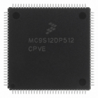
MC9S12DP512CPVER Freescale Semiconductor, MC9S12DP512CPVER Datasheet - Page 79

MC9S12DP512CPVER
Manufacturer Part Number
MC9S12DP512CPVER
Description
IC MCU 16BIT 4K FLASH 112-LQFP
Manufacturer
Freescale Semiconductor
Series
HCS12r
Datasheet
1.MC9S12DP512CPVE.pdf
(124 pages)
Specifications of MC9S12DP512CPVER
Core Processor
HCS12
Core Size
16-Bit
Speed
25MHz
Connectivity
CAN, I²C, SCI, SPI
Peripherals
PWM, WDT
Number Of I /o
91
Program Memory Size
512KB (512K x 8)
Program Memory Type
FLASH
Eeprom Size
4K x 8
Ram Size
12K x 8
Voltage - Supply (vcc/vdd)
2.35 V ~ 5.25 V
Data Converters
A/D 16x10b
Oscillator Type
Internal
Operating Temperature
-40°C ~ 85°C
Package / Case
112-LQFP
Package
112LQFP
Family Name
HCS12
Maximum Speed
25 MHz
Operating Supply Voltage
2.5|5 V
Data Bus Width
16 Bit
Interface Type
CAN/I2C/SCI/SPI
On-chip Adc
2(8-chx10-bit)
Number Of Timers
8
Lead Free Status / RoHS Status
Lead free / RoHS Compliant
Other names
MC9S12DP512CPVERTR
Available stocks
Company
Part Number
Manufacturer
Quantity
Price
Company:
Part Number:
MC9S12DP512CPVER
Manufacturer:
Freescale Semiconductor
Quantity:
10 000
MC9S12DP512 Device Guide V01.25
There are two Analog to Digital Converters (ATD1 and ATD0) implemented on the MC9S12DP512.
Consult the ATD_10B8C Block Guide for information about each Analog to Digital Converter module.
When the ATD_10B8C Block Guide refers to freeze mode this is equivalent to active BDM mode.
Section 11 Inter-IC Bus (IIC) Block Description
Consult the IIC Block Guide for information about the Inter-IC Bus module.
Section 12 Serial Communications Interface (SCI) Block
Description
There are two Serial Communications Interfaces (SCI1 and SCI0) implemented on the MC9S12DP512
device.
Consult the SCI Block Guide for information about each Serial Communications Interface module.
Section 13 Serial Peripheral Interface (SPI) Block
Description
There are three Serial Peripheral Interfaces (SPI2, SPI1 and SPI0) implemented on MC9S12DP512.
Consult the SPI Block Guide for information about each Serial Peripheral Interface module.
Section 14 J1850 (BDLC) Block Description
Consult the BDLC Block Guide for information about the J1850 module.
Section 15 Pulse Width Modulator (PWM) Block
Description
Consult the PWM_8B6C Block Guide for information about the Pulse Width Modulator module.
When the PWM_8B8C Block Guide refers to freeze mode this is equivalent to active BDM mode.
Section 16 Flash EEPROM 512K Block Description
Consult the FTS512K4 Block Guide for information about the flash module.
79


