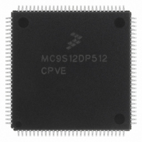
MC9S12DP512CPVER Freescale Semiconductor, MC9S12DP512CPVER Datasheet - Page 3

MC9S12DP512CPVER
Manufacturer Part Number
MC9S12DP512CPVER
Description
IC MCU 16BIT 4K FLASH 112-LQFP
Manufacturer
Freescale Semiconductor
Series
HCS12r
Datasheet
1.MC9S12DP512CPVE.pdf
(124 pages)
Specifications of MC9S12DP512CPVER
Core Processor
HCS12
Core Size
16-Bit
Speed
25MHz
Connectivity
CAN, I²C, SCI, SPI
Peripherals
PWM, WDT
Number Of I /o
91
Program Memory Size
512KB (512K x 8)
Program Memory Type
FLASH
Eeprom Size
4K x 8
Ram Size
12K x 8
Voltage - Supply (vcc/vdd)
2.35 V ~ 5.25 V
Data Converters
A/D 16x10b
Oscillator Type
Internal
Operating Temperature
-40°C ~ 85°C
Package / Case
112-LQFP
Package
112LQFP
Family Name
HCS12
Maximum Speed
25 MHz
Operating Supply Voltage
2.5|5 V
Data Bus Width
16 Bit
Interface Type
CAN/I2C/SCI/SPI
On-chip Adc
2(8-chx10-bit)
Number Of Timers
8
Lead Free Status / RoHS Status
Lead free / RoHS Compliant
Other names
MC9S12DP512CPVERTR
Available stocks
Company
Part Number
Manufacturer
Quantity
Price
Company:
Part Number:
MC9S12DP512CPVER
Manufacturer:
Freescale Semiconductor
Quantity:
10 000
Number
Version
V01.06
V01.07
V01.08
V01.09
V01.10
V01.11
V01.12
V01.13
V01.14
V01.15
Revision
21 Aug
24 Sep
03 Dec
28 Feb
18 Oct
29 Oct
08 Jan
23 Jan
24 Jul
29 Jul
Date
2002
2002
2002
2002
2002
2002
2002
2003
2003
2003
Effective
05 Aug
21 Aug
24 Sep
03 Dec
28 Feb
18 Oct
29 Oct
08 Jan
23 Jan
24 Jul
Date
2002
2002
2002
2002
2002
2002
2002
2003
2003
2003
Author
- Updated SPI electrical characteristics.
- Updated Derivative Differences table.
- Added ordering number example.
- Added Detailed Register Map.
- Changed Internal Pull Resistor column of signal table.
- Added pull device description for MODC pin.
- Corrected XCLKS figure titles. Moved table to section Modes of
Operation.
- Removed ’1/2’ from BDM in Figure Clock Connections.
- Completely reworked section Modes of Operation. Added Chip
Configuration Summary and Low Power Mode description.
- Changed classification to C for internal pull currents inTable 5V I/O
Characteristics.
- Changed input leakage to 1uA for all pins.
- Updated VREG section and layout recommendation.
- Moved Power and Gound Connection Summary table to start of
Power Supply Pins section.
- Added ROMONE to pinout
- Corrected mem map: ’MEBI map x of 3’
- Corrected mem map: KEYEN bits in FSEC.
- Added section Printed Circuit Board Layout Proposal.
- Corrected addresses in Reserved, CAN and EEP buffer map.
- Updated NVM electricals.
- Updated table ’Document References’
- Added section ’Oscillator (OSC) Block Description’
- Section HCS12 Core Block Desciption: mentioned alternalte clock of
BDM to be equivalent to oscillator clock
- Corrected tables 0-1 and 0-2
- Added derivatives to cover sheet.
- Added part ID for 1L00M maskset.
- Corrected in footnote of Table "PLL Characteristics": f
- Renamed Preface section to Derivative Differences and Document
references.
- Added A512 derivative.
- Updated module set of DJ512 in Table 0-1.
- Added details for derivatives without CAN and/or BDLC modules.
- Corrected several entries in ’Detailed Memory Map’.
- Removed footnote on input leakage current from table ’5V I/O
Characteristics’.
- Updated section ’Unsecuring the Microcontroller’.
- Updated footnote 1 in table ’Operating Conditions’.
- Renamed ROMONE pin to ROMCTL.
- Corrected PE[1,0] pull specification in Signal Properties Summary
Table.
Description of Changes
MC9S12DP512 Device Guide V01.25
OSC
= 4MHz.
3


