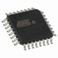
AT90LS4433-4AC Atmel, AT90LS4433-4AC Datasheet - Page 46

AT90LS4433-4AC
Manufacturer Part Number
AT90LS4433-4AC
Description
IC MCU 4K 4MHZ A/D LV 32TQFP
Manufacturer
Atmel
Series
AVR® 90LSr
Datasheet
1.AT90S4433-8AC.pdf
(126 pages)
Specifications of AT90LS4433-4AC
Core Processor
AVR
Core Size
8-Bit
Speed
4MHz
Connectivity
SPI, UART/USART
Peripherals
Brown-out Detect/Reset, POR, PWM, WDT
Number Of I /o
20
Program Memory Size
4KB (2K x 16)
Program Memory Type
FLASH
Eeprom Size
256 x 8
Ram Size
128 x 8
Voltage - Supply (vcc/vdd)
2.7 V ~ 6 V
Data Converters
A/D 6x10b
Oscillator Type
External
Operating Temperature
0°C ~ 70°C
Package / Case
32-TQFP, 32-VQFP
Lead Free Status / RoHS Status
Contains lead / RoHS non-compliant
Available stocks
Company
Part Number
Manufacturer
Quantity
Price
Company:
Part Number:
AT90LS4433-4AC
Manufacturer:
ATM
Quantity:
72
• Bit 3 – EERIE: EEPROM Ready Interrupt Enable
When the I-bit in SREG and EERIE are set (one), the EEPROM Ready Interrupt is
enabled. When cleared (zero), the interrupt is disabled. The EEPROM Ready Interrupt
generates a constant interrupt when EEWE is cleared (zero).
• Bit 2 – EEMWE: EEPROM Master Write Enable
The EEMWE bit determines whether setting EEWE to one causes the EEPROM to be
written. When EEMWE is set (one), setting EEWE will write data to the EEPROM at the
selected address. If EEMWE is zero, setting EEWE will have no effect. When EEMWE
has been set (one) by software, hardware clears the bit to zero after four clock cycles.
See the description of the EEWE bit for a EEPROM write procedure.
• Bit 1 – EEWE: EEPROM Write Enable
The EEPROM Write Enable Signal (EEWE) is the write strobe to the EEPROM. When
address and data are correctly set up, the EEWE bit must be set to write the value into
the EEPROM. The EEMWE bit must be set when the logical “1” is written to EEWE, oth-
erwise no EEPROM write takes place. The following procedure should be followed
when writing the EEPROM (the order of steps 2 and 3 is unessential):
1. Wait until EEWE becomes zero.
2. Write new EEPROM address to EEAR (optional).
3. Write new EEPROM data to EEDR (optional).
4. Write a logical “1” to the EEMWE bit in EECR (to be able to write a logical “1” to
the EEMWE bit, the EEWE bit must be written to zero in the same cycle).
5. Within four clock cycles after setting EEMWE, write a logical “1” to EEWE.
Caution: An interrupt between step 4 and step 5 will make the write cycle fail, since the
EEPROM Master Write Enable will time-out. If an interrupt routine accessing the
EEPROM is interrupting another EEPROM access, the EEAR and EEDR Registers will
be modified, causing the interrupted EEPROM access to fail. It is recommended to have
the global interrupt flag cleared during the last four steps to avoid these problems.
When the write access time (typically 2.5 ms at V
= 5V or 4 ms at V
= 2.7V) has
CC
CC
elapsed, the EEWE bit is cleared (zero) by hardware. The user software can poll this bit
and wait for a zero before writing the next byte. When EEWE has been set, the CPU is
halted for two cycles before the next instruction is executed.
• Bit 0 – EERE: EEPROM Read Enable
The EEPROM Read Enable Signal (EERE) is the read strobe to the EEPROM. When
the correct address is set up in the EEAR Register, the EERE bit must be set. When the
EERE bit is cleared (zero) by hardware, requested data is found in the EEDR Register.
The EEPROM read access takes one instruction and there is no need to poll the EERE
bit. When EERE has been set, the CPU is halted for four cycles before the next instruc-
tion is executed.
The user should poll the EEWE bit before starting the read operation. If a write operation
is in progress when new data or address is written to the EEPROM I/O Registers, the
write operation will be interrupted and the result is undefined.
AT90S/LS4433
46
1042H–AVR–04/03


