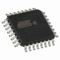
AT90LS4433-4AC Atmel, AT90LS4433-4AC Datasheet - Page 68

AT90LS4433-4AC
Manufacturer Part Number
AT90LS4433-4AC
Description
IC MCU 4K 4MHZ A/D LV 32TQFP
Manufacturer
Atmel
Series
AVR® 90LSr
Datasheet
1.AT90S4433-8AC.pdf
(126 pages)
Specifications of AT90LS4433-4AC
Core Processor
AVR
Core Size
8-Bit
Speed
4MHz
Connectivity
SPI, UART/USART
Peripherals
Brown-out Detect/Reset, POR, PWM, WDT
Number Of I /o
20
Program Memory Size
4KB (2K x 16)
Program Memory Type
FLASH
Eeprom Size
256 x 8
Ram Size
128 x 8
Voltage - Supply (vcc/vdd)
2.7 V ~ 6 V
Data Converters
A/D 6x10b
Oscillator Type
External
Operating Temperature
0°C ~ 70°C
Package / Case
32-TQFP, 32-VQFP
Lead Free Status / RoHS Status
Contains lead / RoHS non-compliant
Available stocks
Company
Part Number
Manufacturer
Quantity
Price
Company:
Part Number:
AT90LS4433-4AC
Manufacturer:
ATM
Quantity:
72
ADC Multiplexer Select
Register – ADMUX
ADC Control and Status
Register – ADCSR
68
AT90S/LS4433
• Bit 7 – Res: Reserved Bit
This bit is a reserved bit in the AT90S4433, and should be written to zero if accessed.
• Bit 6 – ADCBG: ADC Bandgap Select
When this bit is set and the BOD is enabled (BODEN Fuse is programmed), a fixed
bandgap voltage of 1.22V ± 0.1V replaces the normal input to the ADC. When this bit is
cleared, the normal input pin (as selected by MUX2..MUX0) is applied to the ADC.
• Bits 5..3 – Res: Reserved Bits
These bits are reserved bits in the AT90S4433, and should be written to zero if
accessed.
• Bits 2..0 – MUX2..MUX0: Analog Channel Select Bits 2 - 0
The value of these three bits selects which analog input 5 - 0 is connected to the ADC.
‘
• Bit 7 – ADEN: ADC Enable
Writing a logical “1” to this bit enables the ADC. By clearing this bit to zero, the ADC is
turned off. Turning the ADC off while a conversion is in progress will terminate this
conversion.
• Bit 6 – ADSC: ADC Start Conversion
In Single Conversion mode, a logical “1” must be written to this bit to start each conver-
sion. In Free Run mode, a logical “1” must be written to this bit to start the first
conversion. The first time ADSC has been written after the ADC has been enabled, or if
ADSC is written at the same time as the ADC is enabled, a dummy conversion will pre-
cede the initiated conversion. This dummy conversion performs initialization of the ADC.
ADSC remains high during the conversion. ADSC goes low after the conversion is com-
plete, but before the result is written to the ADC Data Registers. This allows a new
conversion to be initiated before the current conversion is complete. The new conver-
sion will then start immediately after the current conversion completes. When a dummy
conversion precedes a real conversion, ADSC will stay high until the real conversion
completes.
Writing a “0” to this bit has no effect.
Bit
$07 ($27)
Read/Write
Initial Value
Bit
$06 ($26)
Read/Write
Initial Value
ADEN
R/W
R
7
–
0
7
0
ADCBG
ADSC
R/W
R/W
6
0
6
0
ADFR
R/W
R
5
0
5
–
0
ADIF
R/W
R
4
0
4
–
0
ADIE
R/W
R
3
0
3
–
0
ADPS2
MUX2
R/W
R/W
2
0
2
0
ADPS1
MUX1
R/W
R/W
1
0
1
0
ADPS0
MUX0
R/W
R/W
0
0
0
0
1042H–AVR–04/03
ADMUX
ADCSR


