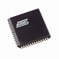
AT89C5131-S3SIL Atmel, AT89C5131-S3SIL Datasheet - Page 115

AT89C5131-S3SIL
Manufacturer Part Number
AT89C5131-S3SIL
Description
IC 8051 MCU FLASH 32K USB 52PLCC
Manufacturer
Atmel
Series
AT89C513xr
Datasheet
1.AT89C5131-S3SIL.pdf
(176 pages)
Specifications of AT89C5131-S3SIL
Core Processor
C52X2
Core Size
8-Bit
Speed
48MHz
Connectivity
I²C, SPI, UART/USART, USB
Peripherals
LED, POR, PWM, WDT
Number Of I /o
34
Program Memory Size
32KB (32K x 8)
Program Memory Type
FLASH
Eeprom Size
4K x 8
Ram Size
1.25K x 8
Voltage - Supply (vcc/vdd)
3 V ~ 3.6 V
Oscillator Type
Internal
Operating Temperature
-40°C ~ 85°C
Package / Case
52-PLCC
For Use With
AT89STK-10 - KIT EVAL APPL MASS STORAGEAT89STK-05 - KIT STARTER FOR AT89C5131
Lead Free Status / RoHS Status
Contains lead / RoHS non-compliant
Data Converters
-
Available stocks
Company
Part Number
Manufacturer
Quantity
Price
- Current page: 115 of 176
- Download datasheet (3Mb)
USB Device Firmware
Upgrade (DFU)
Description
Figure 53. USB Device Controller Block Diagram
4136B–USB–09/03
D+
D-
USB
D+/D-
Buffer
DPLL
The USB Device Firmware Update (DFU) protocol can be used to upgrade the on-chip
Flash memory of the AT89C5131. This allows the implementation of product enhance-
ments and patches to devices that are already in the field. Two different configurations
and descriptor sets are used to support DFU functions. The Run-Time configuration co-
exists with the usual functions of the device, which may be USB Mass Storage for the
AT89C5131. It is used to initiate DFU from the normal operating mode. The DFU config-
uration is used to perform the firmware update after device re-configuration and USB
reset. It excludes any other function. Only the default control pipe (endpoint 0) is used to
support DFU services in both configurations.
The only possible value for the wMaxPacketSize in the DFU configuration is 32 bytes,
which is the size of the FIFO implemented for endpoint 0.
The USB device controller provides the hardware that the AT89C5131 needs to inter-
face a USB link to a data flow stored in a double port memory (DPRAM).
The USB controller requires a 48 MHz ±0.25% reference clock, which is the output of
the AT89C5131 PLL (see Section “PLL”, page 20) divided by a clock prescaler. This
clock is used to generate a 12 MHz Full-speed bit clock from the received USB differen-
tial data and to transmit data according to full speed USB device tolerance. Clock
recovery is done by a Digital Phase Locked Loop (DPLL) block, which is compliant with
the jitter specification of the USB bus.
The Serial Interface Engine (SIE) block performs NRZI encoding and decoding, bit stuff-
ing, CRC generation and checking, and the serial-parallel data conversion.
The Universal Function Interface (UFI) realizes the interface between the data flow and
the Dual Port RAM.
SIE
48 MHz
12 MHz
+/- 0.25%
UFI
C51
Microcontroller
Interface
Up to 48 MHz
UC_sysclk
AT89C5131
115
Related parts for AT89C5131-S3SIL
Image
Part Number
Description
Manufacturer
Datasheet
Request
R

Part Number:
Description:
8-bit Flash Microcontroller With Full Speed Usb Device At89c5131
Manufacturer:
ATMEL Corporation
Datasheet:

Part Number:
Description:
IC 8051 MCU FLASH 32K USB 28SOIC
Manufacturer:
Atmel
Datasheet:

Part Number:
Description:
8-bit Flash Microcontroller with Full Speed USB Device
Manufacturer:
ATMEL Corporation
Datasheet:

Part Number:
Description:
KIT STARTER FOR AT89C5131
Manufacturer:
Atmel
Datasheet:

Part Number:
Description:
IC 8051 MCU FLASH 32K USB 48QFN
Manufacturer:
Atmel
Datasheet:

Part Number:
Description:
IC 8051 MCU FLASH 32K USB 64VQFP
Manufacturer:
Atmel
Datasheet:

Part Number:
Description:
DEV KIT FOR AVR/AVR32
Manufacturer:
Atmel
Datasheet:

Part Number:
Description:
INTERVAL AND WIPE/WASH WIPER CONTROL IC WITH DELAY
Manufacturer:
ATMEL Corporation
Datasheet:

Part Number:
Description:
Low-Voltage Voice-Switched IC for Hands-Free Operation
Manufacturer:
ATMEL Corporation
Datasheet:

Part Number:
Description:
MONOLITHIC INTEGRATED FEATUREPHONE CIRCUIT
Manufacturer:
ATMEL Corporation
Datasheet:

Part Number:
Description:
AM-FM Receiver IC U4255BM-M
Manufacturer:
ATMEL Corporation
Datasheet:

Part Number:
Description:
Monolithic Integrated Feature Phone Circuit
Manufacturer:
ATMEL Corporation
Datasheet:

Part Number:
Description:
Multistandard Video-IF and Quasi Parallel Sound Processing
Manufacturer:
ATMEL Corporation
Datasheet:


