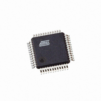
AT91SAM7S32-AU-001 Atmel, AT91SAM7S32-AU-001 Datasheet - Page 540

AT91SAM7S32-AU-001
Manufacturer Part Number
AT91SAM7S32-AU-001
Description
IC ARM7 MCU 32BIT 32K 48LQFP
Manufacturer
Atmel
Series
AT91SAMr
Specifications of AT91SAM7S32-AU-001
Core Processor
ARM7
Core Size
16/32-Bit
Speed
55MHz
Connectivity
I²C, SPI, SSC, UART/USART
Peripherals
Brown-out Detect/Reset, POR, PWM, WDT
Number Of I /o
21
Program Memory Size
32KB (32K x 8)
Program Memory Type
FLASH
Ram Size
8K x 8
Voltage - Supply (vcc/vdd)
1.65 V ~ 1.95 V
Data Converters
A/D 8x10b
Oscillator Type
Internal
Operating Temperature
-40°C ~ 85°C
Package / Case
48-LQFP
For Use With
AT91SAM7S-EK - KIT EVAL FOR ARM AT91SAM7S
Lead Free Status / RoHS Status
Lead free / RoHS Compliant
Eeprom Size
-
Other names
AT91SAM7S32-AU001
Available stocks
Company
Part Number
Manufacturer
Quantity
Price
- Current page: 540 of 779
- Download datasheet (11Mb)
36.5.5
36.5.6
540
AT91SAM7S Series Preliminary
Conversion Triggers
Sleep Mode and Conversion Sequencer
Conversions of the active analog channels are started with a software or a hardware trigger. The
software trigger is provided by writing the Control Register (ADC_CR) with the bit START at 1.
The hardware trigger can be one of the TIOA outputs of the Timer Counter channels, or the
external trigger input of the ADC (ADTRG). The hardware trigger is selected with the field TRG-
SEL in the Mode Register (ADC_MR). The selected hardware trigger is enabled with the bit
TRGEN in the Mode Register (ADC_MR).
If a hardware trigger is selected, the start of a conversion is triggered after a delay starting at
each rising edge of the selected signal. Due to asynchronism handling, the delay may vary in a
range of 2 MCK clock periods to 1 ADC clock period.
If one of the TIOA outputs is selected, the corresponding Timer Counter channel must be pro-
grammed in Waveform Mode.
Only one start command is necessary to initiate a conversion sequence on all the channels. The
ADC hardware logic automatically performs the conversions on the active channels, then waits
for a new request. The Channel Enable (ADC_CHER) and Channel Disable (ADC_CHDR) Reg-
isters enable the analog channels to be enabled or disabled independently.
If the ADC is used with a PDC, only the transfers of converted data from enabled channels are
performed and the resulting data buffers should be interpreted accordingly.
Warning: Enabling hardware triggers does not disable the software trigger functionality. Thus, if
a hardware trigger is selected, the start of a conversion can be initiated either by the hardware or
the software trigger.
The ADC Sleep Mode maximizes power saving by automatically deactivating the ADC when it is
not being used for conversions. Sleep Mode is selected by setting the bit SLEEP in the Mode
Register ADC_MR.
The SLEEP mode is automatically managed by a conversion sequencer, which can automati-
cally process the conversions of all channels at lowest power consumption.
When a start conversion request occurs, the ADC is automatically activated. As the analog cell
requires a start-up time, the logic waits during this time and starts the conversion on the enabled
channels. When all conversions are complete, the ADC is deactivated until the next trigger. Trig-
gers occurring during the sequence are not taken into account.
The conversion sequencer allows automatic processing with minimum processor intervention
and optimized power consumption. Conversion sequences can be performed periodically using
a Timer/Counter output. The periodic acquisition of several samples can be processed automat-
ically without any intervention of the processor thanks to the PDC.
Note:
The reference voltage pins always remain connected in normal mode as in sleep mode.
trigger
start
delay
6175K–ATARM–30-Aug-10
Related parts for AT91SAM7S32-AU-001
Image
Part Number
Description
Manufacturer
Datasheet
Request
R

Part Number:
Description:
Manufacturer:
ATMEL Corporation
Datasheet:

Part Number:
Description:
AT91 ARM Thumb-based Microcontrollers
Manufacturer:
ATMEL [ATMEL Corporation]
Datasheet:

Part Number:
Description:
IC ARM7 MCU FLASH 32K 48QFN
Manufacturer:
Atmel
Datasheet:

Part Number:
Description:
IC MCU ARM7 32KB FLASH 48LQFP
Manufacturer:
Atmel
Datasheet:

Part Number:
Description:
IC MCU ARM7 32KB FLASH 48-VQFN
Manufacturer:
Atmel
Datasheet:

Part Number:
Description:
DEV KIT FOR AVR/AVR32
Manufacturer:
Atmel
Datasheet:

Part Number:
Description:
INTERVAL AND WIPE/WASH WIPER CONTROL IC WITH DELAY
Manufacturer:
ATMEL Corporation
Datasheet:

Part Number:
Description:
Low-Voltage Voice-Switched IC for Hands-Free Operation
Manufacturer:
ATMEL Corporation
Datasheet:

Part Number:
Description:
MONOLITHIC INTEGRATED FEATUREPHONE CIRCUIT
Manufacturer:
ATMEL Corporation
Datasheet:

Part Number:
Description:
AM-FM Receiver IC U4255BM-M
Manufacturer:
ATMEL Corporation
Datasheet:

Part Number:
Description:
Monolithic Integrated Feature Phone Circuit
Manufacturer:
ATMEL Corporation
Datasheet:

Part Number:
Description:
Multistandard Video-IF and Quasi Parallel Sound Processing
Manufacturer:
ATMEL Corporation
Datasheet:


