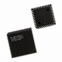
PXAC37KFA/00,512 NXP Semiconductors, PXAC37KFA/00,512 Datasheet - Page 44

PXAC37KFA/00,512
Manufacturer Part Number
PXAC37KFA/00,512
Description
IC XA MCU 16BIT 32K OTP 44-PLCC
Manufacturer
NXP Semiconductors
Series
XAr
Datasheet
1.PXAC37KFA00512.pdf
(68 pages)
Specifications of PXAC37KFA/00,512
Core Processor
XA
Core Size
16-Bit
Speed
32MHz
Connectivity
CAN, EBI/EMI, SPI, UART/USART
Peripherals
DMA, POR, PWM, WDT
Number Of I /o
32
Program Memory Size
32KB (32K x 8)
Program Memory Type
OTP
Ram Size
1K x 8
Voltage - Supply (vcc/vdd)
4.5 V ~ 5.5 V
Oscillator Type
External
Operating Temperature
-40°C ~ 85°C
Package / Case
44-PLCC
Lead Free Status / RoHS Status
Lead free / RoHS Compliant
Eeprom Size
-
Data Converters
-
Other names
568-3533-5
935266516512
PXAC37KFA
935266516512
PXAC37KFA
Available stocks
Company
Part Number
Manufacturer
Quantity
Price
Company:
Part Number:
PXAC37KFA/00,512
Manufacturer:
NXP Semiconductors
Quantity:
10 000
Philips Semiconductors
objects having the same ID. An alternate option bases transmit
pre–arbitration exclusively on transmit object number, i.e.,
independent of arbitration ID.
Remote Frame Handling
The XA-C3 supports Remote CAN Frames.
MEMORY MAPS
Data Memory Space
1K byte of internal data memory (Scratch Pad) populates the very
bottom of data memory space, in Segment 0 by definition. The
Memory Mapped Registers and the on–chip XRAM can also be
mapped into Segment 0 (as shown in Figure 36), or into any other
segment.
Code Memory Space
32K Bytes of Internal Code Memory populate addresses 000000h –
007FFFh of code memory space. As shown in Figure 37, code
2000 Jan 25
4K Bytes
512 Bytes
XA 16-bit microcontroller family
32K/1024 OTP CAN transport layer controller
1 UART, 1 SPI Port, CAN 2.0B, 32 CAN ID filters, transport layer co-processor
Figure 36. MMRs and XRAM mapped into Segment 00h.
00FFFFh
0003FFh
On–Chip Data Memory
Data Memory Segment 0
(Scratch Pad)
MMR Space
Off–Chip
Off–Chip
XRAM
Off–Chip
MMR Base Address
XRAM Base Address
000000h
SU01337
37
memory can be extended off–chip, if desired, starting at address
008000h. The code memory address space extends to 0FFFFFh.
CAN CORE BLOCK (CCB)
CAN Bus Timing
CAN System Clock
The CCB has a programmable internal system clock, whose period
is denoted by tSCL. The CAN System Clock is derived from the XA
Oscillator Clock based on the following expression:
where tCLK is the period of the XA Oscillator Clock, and BRP.5 –
BRP.0 are bits in the MMR CAN Bus Timing Register (CANBTR).
The length of a bit period in a CAN Frame is expressed in terms of
number of CAN System Clocks.
Samples Per Bit
The number of samples per bit is determined by the value of the
SAM bit in CANBTR.
tSCL =2 tCLK
BRP.2 + 2 BRP.1 + BRP.0 + 1)
SAM = 0 The bus is sampled once per bit (as shown below)
SAM = 1 The bus is sampled three times per bit (as shown
below)
0FFFFFh
007FFFh
Figure 37. External Code Memory starts at 008000h.
Internal Code Memory
(32
Code Memory
BRP.5 + 16 BRP.4 + 8 BRP.3 + 4
Off–Chip
Preliminary specification
008000h
000000h
SU01338
XA-C3


