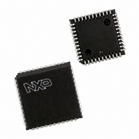
PXAC37KFA/00,512 NXP Semiconductors, PXAC37KFA/00,512 Datasheet - Page 45

PXAC37KFA/00,512
Manufacturer Part Number
PXAC37KFA/00,512
Description
IC XA MCU 16BIT 32K OTP 44-PLCC
Manufacturer
NXP Semiconductors
Series
XAr
Datasheet
1.PXAC37KFA00512.pdf
(68 pages)
Specifications of PXAC37KFA/00,512
Core Processor
XA
Core Size
16-Bit
Speed
32MHz
Connectivity
CAN, EBI/EMI, SPI, UART/USART
Peripherals
DMA, POR, PWM, WDT
Number Of I /o
32
Program Memory Size
32KB (32K x 8)
Program Memory Type
OTP
Ram Size
1K x 8
Voltage - Supply (vcc/vdd)
4.5 V ~ 5.5 V
Oscillator Type
External
Operating Temperature
-40°C ~ 85°C
Package / Case
44-PLCC
Lead Free Status / RoHS Status
Lead free / RoHS Compliant
Eeprom Size
-
Data Converters
-
Other names
568-3533-5
935266516512
PXAC37KFA
935266516512
PXAC37KFA
Available stocks
Company
Part Number
Manufacturer
Quantity
Price
Company:
Part Number:
PXAC37KFA/00,512
Manufacturer:
NXP Semiconductors
Quantity:
10 000
Philips Semiconductors
Location of Sample Point
The location of the sample point within a bit period is determined
according to the following:
CANBTR
CAN Command and Status Registers
Two Modes in CAN Core Operation
The CCB has two different modes of operation: Reset mode, and
Operation mode. On hardware reset, the CAN core is in Reset
mode, and the RR bit of CANCMR (CAN Command Register) will
be set. The User application would usually set up registers, etc.,
then put the CCB into Operation mode by clearing the RR bit.
While in Operation mode, the following conditions will cause the RR
bit to be set, putting the CCB back into Reset mode:
CANCMR
RXP
ST
LO
Reserved
SLPEN
OC1
CANSTR
BS
EP
EW
TS
2000 Jan 25
tSYNCSEG = tSCL
tSEG1 = tSCL
tSEG1.0 + 1)
Tx Buffer Underflow (TBUF)
XA 16-bit microcontroller family
32K/1024 OTP CAN transport layer controller
1 UART, 1 SPI Port, CAN 2.0B, 32 CAN ID filters, transport layer co-processor
SAM
15
RXP
BS
7
7
tSYNC–
TSEG2.2
SEG
14
(8
TSEG2.1
Rx Polarity, writable during reset mode only.
0 = non–inverted, 1 = inverted.
Self test, disable TxACK
Listen only
Reserved bit.
CTL will go back to idle if no interrupt is
generated.
Output control for Tx pad. 0 = Push–Pull,
1 = Open Drain
Bus status
Error passive
Error warning
Transmit status
13
one bit period
tSEG1.3 + 4 tSEG1.2 + 2 tSEG1.1 +
tSEG1
EP
ST
6
6
Sample point
TSEG2.0
12
TSEG1.3
11
tSEG2
EW
LO
5
5
TSEG1.2
10
SU01339
TSEG1.1
9
Reserved
TS
4
4
TSEG1.0
8
38
SJW.1
where tSEG1.3 – tSEG1.0 and tSEG2.2 – tSEG2.0 are bits in
CANBTR.
Synchronization Jump Width
To compensate for phase shifts between clock oscillators of different
bus controllers, any bus controller must re–synchronize on any
relevant signal edge of the current transmission. The
Synchronization Jump Width defines the maximum number of CAN
System Clock cycles that a bit period may be shortened or
lengthened by one re–synchronization, and is given by the following
expression:
where SJW.1 and SJW.0 are bits in CANBTR.
CANBTR: CAN Bus Timing Register
CANCMR: CAN Command Register
Reserved
RR
CANSTR: CAN Status Register
RS
SLPOK
7
SLPEN
tSEG2 = tSCL
tSJW = tSCL
Address: MMR base + 272h
Access: Read, Write during reset mode only. Word access only.
Reset value: 0000h
Bus Off
Hardware reset
Test mode (Refer to XA-C3 User Guide, Sections 2.2.2.1 and
2.7.1.2)
Address: MMR base + 270h
Access: Read/Write, no R/M/W, Byte or Word Access. Hardware
can set bit 0.
Reset value: 01h
Address: MMR base + 271h
Access: Read only, no write, no R/M/W. Byte access OK.
Hardware can set or clear bits 7 – 2.
Reset value: 00h
RS
3
3
SJW.0
6
BRP.5
(2
5
(4
SLPOK
Reserved bit
Reset Request.
Receive status
CAN status: no CAN bus activity and no
pending core interrupts
OC1
SJW.1 + SJW.0 + 1)
2
2
tSEG2.2 + 2 tSEG2.1 + tSEG2.0 + 1)
BRP.4
4
BRP.3
3
Reserved
1
1
–
BRP.2
Preliminary specification
2
BRP.1
XA-C3
1
RR
0
0
–
BRP.0
0


