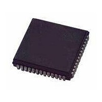
MC68711E20CFNE3 Freescale Semiconductor, MC68711E20CFNE3 Datasheet - Page 32

MC68711E20CFNE3
Manufacturer Part Number
MC68711E20CFNE3
Description
IC MCU 8BIT 52-PLCC
Manufacturer
Freescale Semiconductor
Series
HC11r
Datasheet
1.MC711D3CFNE2R.pdf
(138 pages)
Specifications of MC68711E20CFNE3
Core Processor
HC11
Core Size
8-Bit
Speed
3MHz
Connectivity
SCI, SPI
Peripherals
POR, WDT
Number Of I /o
38
Program Memory Size
20KB (20K x 8)
Program Memory Type
OTP
Eeprom Size
512 x 8
Ram Size
768 x 8
Voltage - Supply (vcc/vdd)
4.5 V ~ 5.5 V
Data Converters
A/D 8x8b
Oscillator Type
Internal
Operating Temperature
-40°C ~ 85°C
Package / Case
52-PLCC
Processor Series
M687xx
Core
HC11
Data Bus Width
8 bit
Data Ram Size
768 B
Interface Type
SCI, SPI
Maximum Clock Frequency
3 MHz
Number Of Programmable I/os
38
Number Of Timers
8
Maximum Operating Temperature
+ 85 C
Mounting Style
SMD/SMT
Minimum Operating Temperature
- 40 C
On-chip Adc
8 bit, 8 Channel
Lead Free Status / RoHS Status
Lead free / RoHS Compliant
Available stocks
Company
Part Number
Manufacturer
Quantity
Price
Company:
Part Number:
MC68711E20CFNE3
Manufacturer:
TI
Quantity:
101
Company:
Part Number:
MC68711E20CFNE3
Manufacturer:
Freescale Semiconductor
Quantity:
10 000
Operating Modes and Memory
2.4.2 Programming the EPROM with Downloaded Data
When using this method, the EPROM is programmed by software while in the special test or bootstrap
modes. User-developed software can be uploaded through the SCI or a ROM-resident EPROM
programming utility can be used. The 12-volt nominal programming voltage must be present on the
XIRQ/V
to $BF00. $BF00 is the starting address of a resident EPROM programming utility. The utility program
sets the X and Y index registers to default values, then receives programming data from an external host,
and puts it in EPROM. The value in IX determines programming delay time. The value in IY is a pointer
to the first address in EPROM to be programmed (default = $F000).
When the utility program is ready to receive programming data, it sends the host the $FF character. Then
it waits. When the host sees the $FF character, the EPROM programming data is sent, starting with the
first location in the EPROM array. After the last byte to be programmed is sent and the corresponding
verification data is returned, the programming operation is terminated by resetting the MCU.
2.4.3 PROM Programming Control Register
The PROM programming control register (PPROG) is used to control the programming of the OTPROM
or EPROM. PPROG is cleared on reset so that the PROM is configured for normal read.
MBE — Multiple Byte Program Enable Bit
Bit 6, 2, and 1 — Not implemented
ELAT — EPROM (OTPROM) Latch Control Bit
EXCOL — Select Extra Columns Bit
EXROW — Select Extra Row Bit
PGM — EPROM (OTPROM) Program Command Bit
32
This bit is reserved for testing.
Always read 0.
This bit is reserved for testing.
This bit is reserved for testing.
This bit may be written only when ELAT = 1.
1 = PROM address and data bus are configured for programming. Writes to PROM cause address
0 = PROM address and data bus are configured for normal reads. PROM cannot be programmed.
1 = Programming power is switched on to PROM array.
0 = Programming power is switched off.
PP
and data to be latched. The PROM cannot be read.
pin. To use the resident utility, bootload a 3-byte program consisting of a single jump instruction
Address: $003B
Reset:
Read:
Write:
Figure 2-5. PROM Programming Control Register (PPROG)
MBE
Bit 7
0
6
0
0
MC68HC711D3 Data Sheet, Rev. 2.1
ELAT
5
0
EXCOL
4
0
EXROW
3
0
2
0
0
1
0
0
Freescale Semiconductor
PGM
Bit 0
0


