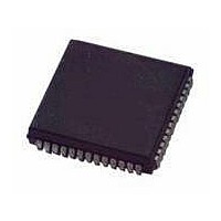
MC68711E20CFNE3 Freescale Semiconductor, MC68711E20CFNE3 Datasheet - Page 96

MC68711E20CFNE3
Manufacturer Part Number
MC68711E20CFNE3
Description
IC MCU 8BIT 52-PLCC
Manufacturer
Freescale Semiconductor
Series
HC11r
Datasheet
1.MC711D3CFNE2R.pdf
(138 pages)
Specifications of MC68711E20CFNE3
Core Processor
HC11
Core Size
8-Bit
Speed
3MHz
Connectivity
SCI, SPI
Peripherals
POR, WDT
Number Of I /o
38
Program Memory Size
20KB (20K x 8)
Program Memory Type
OTP
Eeprom Size
512 x 8
Ram Size
768 x 8
Voltage - Supply (vcc/vdd)
4.5 V ~ 5.5 V
Data Converters
A/D 8x8b
Oscillator Type
Internal
Operating Temperature
-40°C ~ 85°C
Package / Case
52-PLCC
Processor Series
M687xx
Core
HC11
Data Bus Width
8 bit
Data Ram Size
768 B
Interface Type
SCI, SPI
Maximum Clock Frequency
3 MHz
Number Of Programmable I/os
38
Number Of Timers
8
Maximum Operating Temperature
+ 85 C
Mounting Style
SMD/SMT
Minimum Operating Temperature
- 40 C
On-chip Adc
8 bit, 8 Channel
Lead Free Status / RoHS Status
Lead free / RoHS Compliant
Available stocks
Company
Part Number
Manufacturer
Quantity
Price
Company:
Part Number:
MC68711E20CFNE3
Manufacturer:
TI
Quantity:
101
Company:
Part Number:
MC68711E20CFNE3
Manufacturer:
Freescale Semiconductor
Quantity:
10 000
Programmable Timer
8.4.8 Timer Interrupt Flag 1 Register
The timer interrupt flag 1 register (TFLG1) bits indicate when timer system events have occurred. Coupled
with the bits of TMSK1, the bits of TFLG1 allow the timer subsystem to operate in either a polled or
interrupt driven system. Each bit of TFLG1 corresponds to a bit in TMSK1 in the same position.
Clear flags by writing a 1 to the corresponding bit position(s).
OC1F–OC5F — Output Compare x Flag
I4/O5F — Input Capture 4/Output Compare 5 Flag
IC1F–IC3F — Input Capture x Flag
8.4.9 Timer Interrupt Mask 2 Register
The timer interrupt mask 1 register (TMSK2) is an 8-bit register used to enable or inhibit timer overflow
and real-time interrupts. The timer prescaler control bits are included in this register.
TOI — Timer Overflow Interrupt Enable Bit
RTII — Real-Time Interrupt Enable Bit
PAOVI — Pulse Accumulator Overflow Interrupt Enable Bit
PAII — Pulse Accumulator Input Edge Interrupt Enable Bit
96
Set each time the counter matches output compare x value
Set by IC4 or OC5, depending on the function enabled by I4/O5 bit in PACTL
Set each time a selected active edge is detected on the ICx input line
Refer to
Refer to
Refer to
0 = TOF interrupts disabled
1 = Interrupt requested when TOF is set to 1
8.5 Real-Time
8.7 Pulse
8.7 Pulse
Address:
Address:
Bits in TMSK2 correspond bit for bit with flag bits in TFLG2. Ones in TMSK2
enable the corresponding interrupt sources.
Reset:
Reset:
Read:
Read:
Write:
Write:
Accumulator.
Accumulator.
$0023
OC1F
$0024
Bit 7
Bit 7
TOI
Figure 8-14. Timer Interrupt Mask 2 Register (TMSK2)
0
Figure 8-13. Timer Interrupt Flag 1 Register (TFLG1)
0
Interrupt.
OC2F
RTII
6
0
6
0
MC68HC711D3 Data Sheet, Rev. 2.1
PAOVI
OC3F
5
0
5
0
NOTE
OC4F
PAII
4
0
4
0
I4/O5F
3
0
3
0
0
IC1F
2
0
2
0
0
IC2F
PR1
1
0
1
0
Freescale Semiconductor
IC3F
Bit 0
Bit 0
PR0
0
0


