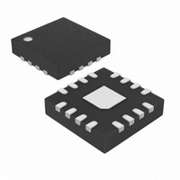
MAX6882ETE+ Maxim Integrated Products, MAX6882ETE+ Datasheet

MAX6882ETE+
Specifications of MAX6882ETE+
Related parts for MAX6882ETE+
MAX6882ETE+ Summary of contents
Page 1
... Nominal IN_/OUT_ Range ♦ 2.7V to 5.5V Operating Voltage Range ♦ Immune to Short Voltage Transients ♦ Small 4mm x 4mm 24-Pin or 16-Pin Thin QFN Packages PART MAX6880ETG+ MAX6881ETE+ MAX6882ETE+ MAX6883ETE+ +Denotes lead-free package. TOP VIEW GATE2 Applications GATE1 *EXPOSED PADDLE CONNECTED TO GND. ...
Page 2
Dual-/Triple-Voltage, Power-Supply Sequencers/Supervisors ABSOLUTE MAXIMUM RATINGS (All voltages referenced to GND, unless otherwise noted.) IN1, IN2, IN3.............................................................-0.3V to +6V ABP .........................................-0.3V to the highest of V SET1, SET2, SET3 ....................................................-0.3V to +6V GATE1, GATE2, GATE3 .........................................-0.3V to +12V OUT1, OUT2, ...
Page 3
Dual-/Triple-Voltage, Power-Supply ELECTRICAL CHARACTERISTICS (continued) (IN1, IN2, or IN3 = +2.7V to +5.5V, EN/UV = MARGIN = ABP +25°C, unless otherwise noted.) (Note 1) A Power-Good Threshold Power-Good Threshold Hysteresis GATE_ Output High GATE_ Pullup Current ...
Page 4
Dual-/Triple-Voltage, Power-Supply Sequencers/Supervisors 125mV DOWN = STOP RAMP THRESHOLD REFERENCE RAMP POWER-UP Figure 1. Stop Ramp/Fault Window During Power-Up and Power-Down EN/UV V EN_R IN1 = 3.3V IN2 = 1.8V IN3 = 0.7V IN_ CAPACITOR- ADJUSTED SLEW RATE OUT_ t ...
Page 5
Dual-/Triple-Voltage, Power-Supply EN/UV V EN_R IN1 = 3.3V IN2 = 1.8V IN3 = 0.7V IN_ CAPACITOR- ADJUSTED SLEW RATE OUT_ t DELAY PG/RST FORCED INTO QUICK SHUTDOWN WHEN OUT1 FALLS BELOW 92.5% of IN1 Figure 3. Sequencing In Fast Shutdown ...
Page 6
Dual-/Triple-Voltage, Power-Supply Sequencers/Supervisors EN/UV BUS VOLTAGE MONITORED THROUGH EN/UV INPUT V EN_R IN1 = 3.3V IN2 = 1.8V IN3 = 0.7V IN_ CAPACITOR- ADJUSTED SLEW RATE OUT_ t DELAY PG/RST = LOW Figure 4. Timing Diagram (Aborted Sequencing) EN/UV V ...
Page 7
Dual-/Triple-Voltage, Power-Supply = 200pF MARGIN = ABP 2.7V to 5.5V, C IN_ SLEW V SUPPLY CURRENT CC vs. INPUT VOLTAGE 1.4 1 +85°C A 1.2 1 +25° ...
Page 8
Dual-/Triple-Voltage, Power-Supply Sequencers/Supervisors = 200pF MARGIN = ABP 2.7V to 5.5V, C IN_ SLEW GATE_ VOLTAGE LOW vs. SINK CURRENT 1.6 1.4 1.2 1.0 0.8 0.6 0.4 0 ...
Page 9
Dual-/Triple-Voltage, Power-Supply PIN MAX6880 MAX6881 MAX6882 1, 11, — — 12 — — — ...
Page 10
Dual-/Triple-Voltage, Power-Supply Sequencers/Supervisors PIN MAX6880 MAX6881 MAX6882 14 — — — — ...
Page 11
Dual-/Triple-Voltage, Power-Supply IN1 MAX6880 SET1 IN2 COMP SET2 IN3 COMP SET3 VBUS COMP EN/UV COMP V MARGIN GND ______________________________________________________________________________________ Sequencers/Supervisors IN2 IN3 IN1 ABP INTERNAL V /UVLO CC RAMP GENERATOR CONTROL LOGIC SEQUENCING MONITOR REF DELAY SLEW C SLEW Functional ...
Page 12
Dual-/Triple-Voltage, Power-Supply Sequencers/Supervisors Detailed Description The MAX6880–MAX6883 multivoltage sequencers/supervisors monitor three (MAX6880/ MAX6881) and two (MAX6882/MAX6883) system volt- ages and provide proper power-up and power-down control for systems requiring voltage sequencing. These devices ensure the controlled voltages sequence in the ...
Page 13
Dual-/Triple-Voltage, Power-Supply reference ramp voltage. During ramp down OUT_ voltage is greater than the reference ramp voltage by more than V , the control loop dynamically stops the TRK control ramp voltage from decreasing until the slow OUT_ ...
Page 14
Dual-/Triple-Voltage, Power-Supply Sequencers/Supervisors Table 1. C Timing Formulas SLEW TIME PERIOD Slew Rate (9. 3.506 x 10 RETRY t 2.191 x 10 FAULT Limiting Inrush Current The capacitor ( SLEW to ground, controls the SLEW ...
Page 15
Dual-/Triple-Voltage, Power-Supply Applications Information MOSFET Selection The external pass MOSFET is connected in series with the sequenced power-supply source. Since the load current and the MOSFET drain-to-source impedance (R ) determine the voltage drop, the on characteris- DS tics of ...
Page 16
Dual-/Triple-Voltage, Power-Supply Sequencers/Supervisors IN1 IN2 IN3 V BUS 16 ______________________________________________________________________________________ Typical Application Circuit 0.1µF 0.1µF 0.1µF IN1 IN2 IN3 GATE1 GATE2 SET1 SET2 MAX6880 SET3 EN/UV ABP SLEW GND DELAY TIMEOUT 1µF OUT1 OUT2 OUT3 GATE3 OUT1 OUT2 OUT3 PG/RST ...
Page 17
Dual-/Triple-Voltage, Power-Supply TOP VIEW OUT1 13 GATE1 14 MAX6881 IN3 15 EP* IN2 4mm x 4mm THIN QFN *EXPOSED PADDLE CONNECTED TO GND. ______________________________________________________________________________________ Sequencers/Supervisors Pin Configurations (continued) SLEW 8 ...
Page 18
Dual-/Triple-Voltage, Power-Supply Sequencers/Supervisors (The package drawing(s) in this data sheet may not reflect the most current specifications. For the latest package outline information www.maxim-ic.com/packages.) 18 ______________________________________________________________________________________ Package Information PACKAGE OUTLINE, 12, 16, 20, 24, 28L THIN QFN, 4x4x0.8mm ...
Page 19
... Maxim cannot assume responsibility for use of any circuitry other than circuitry entirely embodied in a Maxim product. No circuit patent licenses are implied. Maxim reserves the right to change the circuitry and specifications without notice at any time. Maxim Integrated Products, 120 San Gabriel Drive, Sunnyvale, CA 94086 408-737-7600 ____________________ 19 © 2005 Maxim Integrated Products ...


