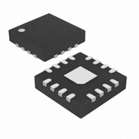
MAX6882ETE+ Maxim Integrated Products, MAX6882ETE+ Datasheet - Page 12

MAX6882ETE+
Manufacturer Part Number
MAX6882ETE+
Description
IC SEQUENCE/SUPERVISOR 16TQFN
Manufacturer
Maxim Integrated Products
Type
Sequencerr
Datasheet
1.MAX6880ETG.pdf
(19 pages)
Specifications of MAX6882ETE+
Number Of Voltages Monitored
2
Output
Open Drain or Open Collector
Reset
Active Low
Reset Timeout
Adjustable/Selectable
Voltage - Threshold
Adjustable/Selectable
Operating Temperature
-40°C ~ 85°C
Mounting Type
Surface Mount
Package / Case
16-TQFN Exposed Pad
Monitored Voltage
- 0.3 V to + 6 V
Manual Reset
Resettable
Watchdog
No Watchdog
Supply Voltage (max)
5.5 V
Supply Voltage (min)
2.7 V
Supply Current (typ)
1100 uA
Maximum Power Dissipation
1349 mW
Maximum Operating Temperature
+ 85 C
Mounting Style
SMD/SMT
Minimum Operating Temperature
- 40 C
Lead Free Status / RoHS Status
Lead free / RoHS Compliant
The
sequencers/supervisors monitor three (MAX6880/
MAX6881) and two (MAX6882/MAX6883) system volt-
ages and provide proper power-up and power-down
control for systems requiring voltage sequencing. These
devices ensure the controlled voltages sequence in the
proper order as system power supplies are enabled.
The MAX6880–MAX6883 generate all required voltages
and timing to control up to three external n-channel
pass FETs for the OUT1/OUT2/OUT3 supply voltages.
The MAX6880–MAX6883 feature adjustable undervolt-
age thresholds for each input supply. When all of the
voltages are above the adjusted thresholds these
devices turn on the external n-channel MOSFETs to
sequence the voltages to the system. The outputs are
turned on one after the other, OUT1 first and OUT3 last.
The MAX6880–MAX6883 feature internal charge pumps
to fully enhance the external FETs for low-voltage drops
at highpass currents. The MAX6880/MAX6882 also fea-
ture a power-good output (PG/RST) with a selectable
timeout period that can be used for system reset.
The MAX6880–MAX6883 monitor up to three voltages.
Devices may be configured to exclude any IN_. To dis-
able sequencing operation of any IN_, connect the IN_
to ground (or leave unconnected) and connect SET_ to
a voltage greater than 0.5V. The channel exclusion fea-
ture adds more flexibility to the device in a variety of
different applications. As an example, the MAX6880
can sequence two voltages using IN1 and IN2 while
IN3 is left disabled.
These devices derive power from either IN1, IN2, or IN3
voltage inputs (see the Functional Diagram). In order to
ensure proper operation, at least one of the IN_ inputs
must be at least +2.7V.
The highest input voltage on IN1/IN2/IN3 supplies
power to the devices. Internal hysteresis ensures that
the supply input that initially powers these devices con-
tinues to power the MAX6880–MAX6883 when multiple
input voltages are within 100mV (typ) of each other.
The sequencing operation can be initiated after all
input conditions for power-up are met V
and all SET_ inputs are above the internal SET_ thresh-
old (0.5V). In sequencing mode, the outputs are turned
on sequentially, OUT1 first and OUT3 last. Before turn-
ing on each channel, a delay period is waited (pro-
grammable by connecting a capacitor from DELAY to
ground. The power-up phase for each channel ends
Dual-/Triple-Voltage, Power-Supply
Sequencers/Supervisors
12
______________________________________________________________________________________
MAX6880–MAX6883
Powering the MAX6880–MAX6883
Detailed Description
multivoltage
Sequencing
EN/UV
> 1.25V
power
when its output voltage exceeds a fixed percentage
(V
channels have exceeded these thresholds, PG/RST
asserts high after t
sequence.
If there is a fault condition during the initial power-up
sequence, the process is aborted.
When powering down, all outputs turn off simultaneous-
ly, tracking each other. No reverse power-down
sequencing occurs.
The power-supply sequencing operation should be
completed within the selected fault timeout period
(t
extended when the devices must vary the control slew
rate to allow slow supplies to catch up. If the external
FET is too small (R
current and IN_ source current), the OUT_ voltage may
never reach the control ramp voltage. For a slew rate of
935V/s, a fault is signaled if all outputs have not stabi-
lized within 22ms. For a slew rate of 93.5V/s, a fault is
signaled if sequencing takes too long (more than
219ms).
The fault time period (t
tor at SLEW (C
mate the fault timeout period:
The MAX6880/MAX6881/MAX6882 feature autoretry
modes to power-on again after a fault condition has been
detected (see the Typical Operating Characteristics).
When a fault is detected, for a period of t
remains off and the 100Ω pulldowns are turned on.
After the t
retry sequencing if all power-up conditions are met
(see Figure 5). These include all V
V
period t
During power-up, OUT_ is forced to follow the internal
reference ramp voltage by an internal loop that controls
the GATE_ of the external MOSFET. This phase must
be completed within the adjustable fault timeout period
(t
GATE_.
Once the power-up is completed, a power-down phase
can be initiated by forcing V
reference voltage ramp ramps down at the capacitor-
adjusted slew rate. The control-loop comparators moni-
tor each OUT_ voltage with respect to the common
FAULT
EN_R
FAULT
TH_PG
, and OUT_ voltages < V
); otherwise, the part forces a shutdown on all
) (see Figure 5). The total sequencing time is
RETRY
) of the corresponding IN_ voltage. When all
RETRY
t
FAULT
is a function of C
SLEW
period, the device waits t
DS
= 2.191 x 10
). Use the following formula to esti-
TIMEOUT
Power-Up and Power-Down
FAULT
is too high for the selected load
) is set through the capaci-
, indicating a successful
EN/UV
SLEW
Autoretry Function
8
TH_PL
SET_
x C
(see Table 1).
below V
SLEW
> 0.5V, EN/UV >
. The autoretry
RETRY
DELAY
EN_F
, GATE_
. The
and


