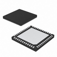
MAX16031ETM+ Maxim Integrated Products, MAX16031ETM+ Datasheet - Page 3

MAX16031ETM+
Manufacturer Part Number
MAX16031ETM+
Description
IC SYSTEM MON EEPROM 48-TQFN
Manufacturer
Maxim Integrated Products
Type
Multi-Voltage Supervisorr
Datasheet
1.MAX16032ETMT.pdf
(41 pages)
Specifications of MAX16031ETM+
Number Of Voltages Monitored
8
Output
Open Drain or Open Collector
Reset
Active Low
Reset Timeout
Adjustable/Selectable
Voltage - Threshold
8 Selectable Threshold Combinations
Operating Temperature
-40°C ~ 85°C
Mounting Type
Surface Mount
Package / Case
48-TQFN Exposed Pad
Manual Reset
Resettable
Watchdog
No Watchdog
Supply Voltage (max)
14 V
Supply Voltage (min)
2.9 V
Supply Current (typ)
3000 uA
Maximum Power Dissipation
2222.2 mW
Maximum Operating Temperature
+ 85 C
Mounting Style
SMD/SMT
Minimum Operating Temperature
- 40 C
Lead Free Status / RoHS Status
Lead free / RoHS Compliant
ABSOLUTE MAXIMUM RATINGS
V
IN_, FAULT_, SCL, SDA, OVERT to GND.................-0.3V to +6V
A0, A1, TCK, TMS, TDI to GND ................................-0.3V to +6V
OVERC, RESET, GPIO_, ALERT to GND..................-0.3V to +6V
RBP, ABP, DBP to GND ...-0.3V to lower of (6V and V
TDO, DXP1, DXP2 to GND..........................-0.3V to V
CS+, CS- to GND ...................................................-0.3V to +30V
(CS+ - CS-) ............................................................................±5V
DXN1, DXN2 to GND.............................................-0.3V to +0.8V
SDA, ALERT Current ...........................................-1mA to +50mA
DXN1, DXN2 Current ............................................................1mA
ELECTRICAL CHARACTERISTICS
(V
Stresses beyond those listed under “Absolute Maximum Ratings” may cause permanent damage to the device. These are stress ratings only, and functional
operation of the device at these or any other conditions beyond those indicated in the operational sections of the specifications is not implied. Exposure to
absolute maximum rating conditions for extended periods may affect device reliability.
Operating Voltage Range
Undervoltage Lockout
Undervoltage Lockout Hysteresis
Supply Current
ADC DC ACCURACY
Resolution
Total Unadjusted Error
Integral Nonlinearity
Differential Nonlinearity
ADC Total Monitoring Cycle Time
ADC IN_ Voltage Ranges
Reference Voltage
IN_ ANALOG INPUT
Absolute Input Voltage Range
(Referenced to GND)
Input Impedance
CC
CC
to GND ............................................................-0.3V to +15V
= 2.9V to 14V, T
PARAMETER
_______________________________________________________________________________________
A
= -40°C to +85°C, unless otherwise specified. Typical values are at V
V
SYMBOL
UVLOHYS
t
V
CYCLE
V
V
UVLO
I
CC
RBP
CC
EEPROM-Based System Monitors
with Nonvolatile Fault Memory
Minimum voltage at V
to access the digital interfaces
Static (EEPROM not accessed)
T
Eight supply inputs, three temperatures,
and current sense
Register map bit set to 00
(LSB = 5.46mV)
Register map bit set to 01
(LSB = 2.73mV)
Register map bit set to 10
(LSB = 1.36mV)
A
DBP
CC
= -40°C to +85°C
+ 0.3V)
+ 0.3V
CONDITIONS
Input/Output Current
Continuous Power Dissipation (T
Operating Temperature Range ...........................-40°C to +85°C
Junction Temperature .....................................................+150°C
Storage Temperature Range .............................-65°C to +150°C
Lead Temperature (soldering, 10s) .................................+250°C
Soldering Temperature (reflow) .......................................+260°C
CC
(all except DXN1, DXN2, SDA, and ALERT) ..................20mA
48-Pin, 7mm x 7mm TQFN
(derate 27.8mW/°C above +70°C) ........................2222.2mW
CC
= 3.3V, T
1.386
MIN
2.90
30
0
A
= +70°C)
A
= +25°C.) (Note 1)
TYP
100
5.6
2.8
1.4
1.4
80
50
3
1
1
14.00
1.414
MAX
100
2.8
0.9
5.6
10
80
5
UNITS
% FSR
LSB
LSB
Bits
mV
mA
kΩ
µs
V
V
V
V
V
3


