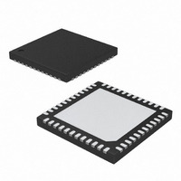
MAX16031ETM+ Maxim Integrated Products, MAX16031ETM+ Datasheet - Page 39

MAX16031ETM+
Manufacturer Part Number
MAX16031ETM+
Description
IC SYSTEM MON EEPROM 48-TQFN
Manufacturer
Maxim Integrated Products
Type
Multi-Voltage Supervisorr
Datasheet
1.MAX16032ETMT.pdf
(41 pages)
Specifications of MAX16031ETM+
Number Of Voltages Monitored
8
Output
Open Drain or Open Collector
Reset
Active Low
Reset Timeout
Adjustable/Selectable
Voltage - Threshold
8 Selectable Threshold Combinations
Operating Temperature
-40°C ~ 85°C
Mounting Type
Surface Mount
Package / Case
48-TQFN Exposed Pad
Manual Reset
Resettable
Watchdog
No Watchdog
Supply Voltage (max)
14 V
Supply Voltage (min)
2.9 V
Supply Current (typ)
3000 uA
Maximum Power Dissipation
2222.2 mW
Maximum Operating Temperature
+ 85 C
Mounting Style
SMD/SMT
Minimum Operating Temperature
- 40 C
Lead Free Status / RoHS Status
Lead free / RoHS Compliant
USERCODE: When the USERCODE instruction is
latched into the parallel instruction register, the user-
code data register is selected. The device user code is
loaded into the user-code data register on the rising
edge of TCK following entry into the capture-DR state.
Shift-DR is used to shift the user code out serially
through TDO. See Table 18.
LOAD ADDRESS: This is an extension to the standard
IEEE 1149.1 instruction set to support access to the
memory in the MAX16031/MAX16032. When the LOAD
ADDRESS instruction is latched into the instruction reg-
ister, TDI connects to TDO through the 8-bit memory
address test data register during the shift-DR state.
READ: This is an extension to the standard IEEE
1149.1 instruction set to support access to the memory
in the MAX16031/MAX16032. When the READ instruc-
tion is latched into the instruction register, TDI connects
to TDO through the 8-bit memory read test data register
during the shift-DR state.
WRITE: This is an extension to the standard IEEE
1149.1 instruction set to support access to the memory
in the MAX16031/MAX16032. When the WRITE instruc-
tion is latched into the instruction register, TDI connects
to TDO through the 8-bit memory write test data regis-
ter during the shift-DR state.
REBOOT: This is an extension to the standard IEEE
1149.1 instruction set to initiate a software-controlled
reset to the MAX16031/MAX16032. When the REBOOT
instruction is latched into the instruction register, the
MAX16031/MAX16032 reset and immediately begin
their boot-up sequence.
Table 17. 32-Bit Identification Code
Table 18. 32-Bit User-Code Data
MSB
MSB
00000000000000000
D.C. (don’t cares)
Version (4 bits)
0000
______________________________________________________________________________________
Slave Address
See Table 15
I
2
C/SMBus
0000000000000001
Device ID (16 bits)
EEPROM-Based System Monitors
r5Eh[7:0] contents
User identification
(firmware version)
with Nonvolatile Fault Memory
SAVE: This is an extension to the standard IEEE 1149.1
instruction set that triggers a fault log. When the SAVE
instruction is latched into the instruction register, the
MAX16031/MAX16032 copy fault information from reg-
isters to EEPROM.
The boundary scan feature allows access to all the dig-
ital I/O connections of the MAX16031/MAX16032. If the
sample/preload or the EXTEST instruction is loaded into
the instruction register, TDI connects to TDO through
the 198-bit boundary scan register. Each digital I/O pin
corresponds to 1 bit (or 2 bits, in the case of the A0
and A1 pins) of the boundary scan register. The rest of
the boundary scan bits are reserved and are loaded
with zeros.
When the sample/preload instruction is executed, the
current state of the digital outputs is latched into the
boundary scan register and is shifted out through TDO.
This instruction may be executed without interrupting
normal operation of the part. When the EXTEST instruc-
tion is executed, the boundary scan register bits super-
sede the normal functionality of the I/O pins: an output
mirrors the state of the corresponding boundary scan
register bit.
Table 19 lists the function of each boundary scan regis-
ter bit. Since the I
possible states, 2 boundary scan register bits are
required to represent them. These bits are defined in
Table 20.
Bypass V
to GND. Bypass RBP with a 2.2µF capacitor to GND.
Avoid routing digital return currents through a sensitive
analog area, such as an analog supply input return
path or ABP’s bypass capacitor ground connection.
Use dedicated analog and digital ground planes.
Manufacturer ID (11 bits)
00011001011
CC
, DBP, and ABP each with a 1µF capacitor
Applications Information
2
C address select pins have three
Layout and Bypassing
Fixed value (1 bit)
Boundary Scan
1
LSB
39


