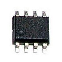
BD3951F-E2 Rohm Semiconductor, BD3951F-E2 Datasheet - Page 4

BD3951F-E2
Manufacturer Part Number
BD3951F-E2
Description
IC REG LDO W/VOLT DETECT 8SOP
Manufacturer
Rohm Semiconductor
Specifications of BD3951F-E2
Regulator Topology
Positive Fixed
Voltage - Output
5V
Voltage - Input
6 ~ 20 V
Voltage - Dropout (typical)
0.31V @ 100mA
Number Of Regulators
1
Current - Output
150mA (Min)
Operating Temperature
-40°C ~ 125°C
Mounting Type
Surface Mount
Package / Case
8-SOP
Primary Input Voltage
13.5V
Output Voltage
5.1V
Dropout Voltage Vdo
310mV
No. Of Pins
8
Output Current
150mA
Voltage Regulator Case Style
SOP
Operating Temperature Range
-40°C To +125°C
Svhc
No
Mounting Style
SMD/SMT
Output Voltage Fixed
5.1V
Rohs Compliant
Yes
Lead Free Status / RoHS Status
Lead free / RoHS Compliant
Current - Limit (min)
-
Lead Free Status / Rohs Status
Lead free / RoHS Compliant
Available stocks
Company
Part Number
Manufacturer
Quantity
Price
Part Number:
BD3951F-E2
Manufacturer:
ROHM/罗姆
Quantity:
20 000
●Block Diagram, Application Circuit, Pin Description
●Terminal Description
BD3951F
© 2009 ROHM Co., Ltd. All rights reserved.
www.rohm.com
RESET function can be discarded while RADJ terminal pulls up to OUT terminal, which in case RES terminal output “H”.
Battery detection function can be discarded while SIN terminal pulls up to OUT terminal, which in case SOUT terminal output
“H”. 0~47KΩ pull up resistors are recommended in both condition.
right pull up resistor value.
・
・
・
R1:10kΩ
Pin. No
R2:36kΩ
0.33μF
ESR range of the output capacitor Co is 0 (ceramic capacitor) to 100Ω.
VCC must be more than 5V under the condition SIN is used for VCC voltage drop detection.
Reset detection voltage must be more than 4V under the condition RADJ is used for OUT voltage drop detection.
1
2
3
4
5
6
7
8
Ex. Vcc=5.8V detection, Since 1.26V*(R1+R2)/R1=5.8V,
RADJ
Ex. OUT=4.5V detection, Since 1.26V*(R3+R4)/R3=4.5V,
Vcc
GND
SIN
3
2
1
5
OUT
(8PIN)
R1=10kΩ,R2=36kΩ
R3=10kΩ,R4=26kΩ
PreReg
VCC
VCC
Pin Name
SOUT
RADJ
GND
OUT
RES
Vcc
SIN
CT
Vref
3.3μF
Fig.13
Battery power supply
Battery voltage detection input terminal. Must be connected to OUT terminal while this
function is not employed.
RESET voltage adjustment terminal. Connect to GND in case internal detect voltage is
employed
RESET delay time control terminal
IC GND terminal
RESET output terminal. Built in 20KΩ pull up.
Battery voltage detection output terminal. Built in 20KΩ pull up.
5.0V output terminal
R
R
4
3
=26kΩ
=10kΩ
20kΩ
20kΩ
8
6
4
7
OUT
CT
RES
SOUT
0.1μF
RADJ
(3PIN)
3.3μF
4/9
OUT SOUT RES GND
Vcc
RADJ
OUT
PIN
Vcc
SIN
CT
SIN RADJ CT
Set application board test is necessary to select the
Function
External
Component
Resistor :R3,R4
Resistor :R1,R2
Capacitor :Cin
Capacitor :Cct
Capacitor :Co
Fig.14
0.01μF~10μF
0Ω~100kΩ
0Ω~100kΩ
Technical Note
2009.07 - Rev.A
0.33μF~
3.3μF~
2200μF
10mF
Value


