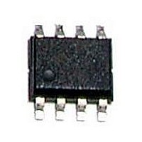
BD3951F-E2 Rohm Semiconductor, BD3951F-E2 Datasheet - Page 8

BD3951F-E2
Manufacturer Part Number
BD3951F-E2
Description
IC REG LDO W/VOLT DETECT 8SOP
Manufacturer
Rohm Semiconductor
Specifications of BD3951F-E2
Regulator Topology
Positive Fixed
Voltage - Output
5V
Voltage - Input
6 ~ 20 V
Voltage - Dropout (typical)
0.31V @ 100mA
Number Of Regulators
1
Current - Output
150mA (Min)
Operating Temperature
-40°C ~ 125°C
Mounting Type
Surface Mount
Package / Case
8-SOP
Primary Input Voltage
13.5V
Output Voltage
5.1V
Dropout Voltage Vdo
310mV
No. Of Pins
8
Output Current
150mA
Voltage Regulator Case Style
SOP
Operating Temperature Range
-40°C To +125°C
Svhc
No
Mounting Style
SMD/SMT
Output Voltage Fixed
5.1V
Rohs Compliant
Yes
Lead Free Status / RoHS Status
Lead free / RoHS Compliant
Current - Limit (min)
-
Lead Free Status / Rohs Status
Lead free / RoHS Compliant
Available stocks
Company
Part Number
Manufacturer
Quantity
Price
Part Number:
BD3951F-E2
Manufacturer:
ROHM/罗姆
Quantity:
20 000
BD3951F
© 2009 ROHM Co., Ltd. All rights reserved.
www.rohm.com
10. Output capacitor between output terminal and GND must be used to prevent undesirable oscillation. Ceramic Capacitor
11. BD3951F might be damaged from the exceed inflow current from the terminals to VCC (for instance, VCC is short to
12. The over-current protection circuits are built in at the output to prevent the IC from being damaged when the load is
13. BD3951F has thermal Shut Down protection (TSD) which performs Power Tr OFF in high Tj condition. If Tj increase
14. Bypass capacitor 0.33μF~10mF into the nearest position between VCC pin and GND is recommended.
15. Insert power zenner diode between VCC terminal and GND terminal is necessary, if more than 50V serge voltage would
16. The SOUT terminal is only activated (“H”/“L”) while the RESET is “H”. While the RESET terminal is “L”, the SOUT
3.3μF~2200μF can be used. When selecting the value of the output capacitor, please make sure that the operation
on the actual application takes these conditions into account: rapid input or load transient response.
GND while the output capacitor is charging.). In those cases, VCC series diode (to prevent inflow current) or bypass
diode (connected from terminals to VCC) should be used externally in an application.
short-circuited or over-current. This protection circuit is droop type and designed not to latch-up in an unexpected huge
current driven.
more than TSD temperature, output power transistor would OFF. After Tj cooled down, the device would be recovered
automatically. This function is designed for to protect the device at the accidental unexpected conditions. Since TSD
setting is higher temperature than absolute maximum ratings, thermal design must has done not to use this function.
be supplied to VCC terminals.
terminal is always “L”.
8/9
Technical Note
2009.07 - Rev.A


