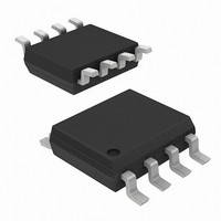
AD8361ARM Analog Devices Inc, AD8361ARM Datasheet - Page 14

AD8361ARM
Manufacturer Part Number
AD8361ARM
Description
IC PWR DETECTOR 2.5GHZ 8-MSOP
Manufacturer
Analog Devices Inc
Datasheet
1.AD8361-EVAL.pdf
(24 pages)
Specifications of AD8361ARM
Rf Type
Cellular, CDMA, W-CDMA
Rohs Status
RoHS non-compliant
Frequency
100MHz ~ 2.5GHz
Input Range
0 ~ 700mV
Accuracy
±0.25dB
Voltage - Supply
2.7 V ~ 5.5 V
Current - Supply
1.1mA
Package / Case
8-TSSOP, 8-MSOP (0.118", 3.00mm Width)
Frequency Range
100MHz To 2.5GHz
Supply Current
1.1mA
Supply Voltage Range
2.7V To 5.5V
Rf Ic Case Style
MSOP
No. Of Pins
8
Operating Temperature Range
-40°C To +85°C
Pin Count
8
Screening Level
Industrial
Package Type
MSOP
Lead Free Status / Rohs Status
Not Compliant
Available stocks
Company
Part Number
Manufacturer
Quantity
Price
Company:
Part Number:
AD8361ARM
Manufacturer:
AD
Quantity:
4 130
Part Number:
AD8361ARM
Manufacturer:
ADI/亚德诺
Quantity:
20 000
Company:
Part Number:
AD8361ARM-REEL7
Manufacturer:
AD
Quantity:
5 321
Company:
Part Number:
AD8361ARMZ
Manufacturer:
ADI
Quantity:
3 000
Company:
Part Number:
AD8361ARMZ
Manufacturer:
SOP8
Quantity:
4 800
Part Number:
AD8361ARMZ
Manufacturer:
ADI/亚德诺
Quantity:
20 000
Part Number:
AD8361ARMZ-REEL
Manufacturer:
ADI/亚德诺
Quantity:
20 000
Part Number:
AD8361ARMZ-REEL7
Manufacturer:
ADI/亚德诺
Quantity:
20 000
Part Number:
AD8361ARMZ-RL7
Manufacturer:
ADI/亚德诺
Quantity:
20 000
AD8361
Table 5. Recommended Component Values for Resistive or
Inductive Input Matching (Figure 43 and Figure 44)
Frequency
100 MHz
800 MHz
900 MHz
1800 MHz
1900 MHz
2500 MHz
Alternatively, a reactive match can be implemented using a shunt
inductor to ground and a series capacitor, as shown in Figure 45. A
method for hand calculating the appropriate matching components
is shown on page 12 of the
Matching in this manner results in very small values for C
especially at high frequencies. As a result, a stray capacitance as
small as 1 pF can significantly degrade the quality of the match.
The main advantage of a reactive match is the increase in
sensitivity that results from the input voltage being gained up
(by the square root of the impedance ratio) by the matching
network. Table 6 shows the recommended values for reactive
matching.
Figure 45. Input Coupling/Matching Options, Narrowband Reactive Match
Figure 46. Input Coupling/Matching Options, Attenuating the Input Signal
Figure 43. Input Coupling/Matching Options, Broadband Resistor Match
Figure 44. Input Coupling/Matching Options, Series Inductor Match
RFIN
RFIN
RFIN
RFIN
Matching Component
63.4 Ω Shunt
75 Ω Shunt
75 Ω Shunt
150 Ω Shunt or 4.7 nH Series
150 Ω Shunt or 4.7 nH Series
150 Ω Shunt or 2.7 nH Series
R
SERIES
L
C
M
M
AD8306
R
SH
L
M
C
C
C
C
data sheet.
C
C
C
C
AD8361
AD8361
AD8361
AD8361
RFIN
RFIN
RFIN
RFIN
M
,
Rev. C | Page 14 of 24
Table 6. Recommended Values for a Reactive Input
Matching (Figure 45)
Frequency (MHz)
100
800
900
1800
1900
2500
Input Coupling Using a Series Resistor
Figure 46 shows a technique for coupling the input signal into
the AD8361 that may be applicable where the input signal is
much larger than the input range of the AD8361. A series
resistor combines with the input impedance of the AD8361 to
attenuate the input signal. Because this series resistor forms a
divider with the frequency dependent input impedance, the
apparent gain changes greatly with frequency. However, this
method has the advantage of very little power being tapped off
in RF power transmission applications. If the resistor is large
compared to the transmission line’s impedance, then the VSWR
of the system is relatively unaffected.
Selecting the Filter Capacitor
The AD8361’s internal 27 pF filter capacitor is connected in
parallel with an internal resistance that varies with signal level
from 2 kΩ for small signals to 500 Ω for large signals. The
resulting low-pass corner frequency between 3 MHz and
12 MHz provides adequate filtering for all frequencies above
240 MHz (i.e., 10 times the frequency at the output of the
squarer, which is twice the input frequency). However, signals
with high peak-to-average ratios, such as CDMA or W-CDMA
signals, and low frequency components require additional
filtering. TDMA signals, such as GSM, PDC, or PHS, have a
peak-to average ratio that is close to that of a sinusoid, and the
internal filter is adequate.
250
200
150
100
50
0
0
Figure 47. Input Impedance vs. Frequency, Supply 3 V, SOT-23
500
1000
FREQUENCY (MHz)
1500
2000
C
16
2
2
1.5
1.5
1.5
M
(pF)
2500
3000
L
180
15
12
4.7
4.7
3.3
M
3500
(nH)
1.7
1.4
1.1
0.8
0.5
0.2


