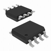
AD8361ARM Analog Devices Inc, AD8361ARM Datasheet - Page 5

AD8361ARM
Manufacturer Part Number
AD8361ARM
Description
IC PWR DETECTOR 2.5GHZ 8-MSOP
Manufacturer
Analog Devices Inc
Datasheet
1.AD8361-EVAL.pdf
(24 pages)
Specifications of AD8361ARM
Rf Type
Cellular, CDMA, W-CDMA
Rohs Status
RoHS non-compliant
Frequency
100MHz ~ 2.5GHz
Input Range
0 ~ 700mV
Accuracy
±0.25dB
Voltage - Supply
2.7 V ~ 5.5 V
Current - Supply
1.1mA
Package / Case
8-TSSOP, 8-MSOP (0.118", 3.00mm Width)
Frequency Range
100MHz To 2.5GHz
Supply Current
1.1mA
Supply Voltage Range
2.7V To 5.5V
Rf Ic Case Style
MSOP
No. Of Pins
8
Operating Temperature Range
-40°C To +85°C
Pin Count
8
Screening Level
Industrial
Package Type
MSOP
Lead Free Status / Rohs Status
Not Compliant
Available stocks
Company
Part Number
Manufacturer
Quantity
Price
Company:
Part Number:
AD8361ARM
Manufacturer:
AD
Quantity:
4 130
Part Number:
AD8361ARM
Manufacturer:
ADI/亚德诺
Quantity:
20 000
Company:
Part Number:
AD8361ARM-REEL7
Manufacturer:
AD
Quantity:
5 321
Company:
Part Number:
AD8361ARMZ
Manufacturer:
ADI
Quantity:
3 000
Company:
Part Number:
AD8361ARMZ
Manufacturer:
SOP8
Quantity:
4 800
Part Number:
AD8361ARMZ
Manufacturer:
ADI/亚德诺
Quantity:
20 000
Part Number:
AD8361ARMZ-REEL
Manufacturer:
ADI/亚德诺
Quantity:
20 000
Part Number:
AD8361ARMZ-REEL7
Manufacturer:
ADI/亚德诺
Quantity:
20 000
Part Number:
AD8361ARMZ-RL7
Manufacturer:
ADI/亚德诺
Quantity:
20 000
PIN CONFIGURATION AND FUNCTION DESCRIPTIONS
Table 3. Pin Function Descriptions
Pin No.
MSOP
1
2
3
4
5
6
7
8
Pin No.
SOT-23
6
N/A
5
4
2
3
1
N/A
PWDN
VPOS
IREF
RFIN
1
2
3
4
Mnemonic
VPOS
IREF
RFIN
PWDN
COMM
FLTR
VRMS
SREF
Figure 4. 8-Lead MSOP
(Not to Scale)
AD8361
TOP VIEW
Description
Supply Voltage Pin. Operational range 2.7 V to 5.5 V.
Output Reference Control Pin. Internal reference mode enabled when pin is left open; otherwise, this
pin should be tied to VPOS. Do not ground this pin.
Signal Input Pin. Must be driven from an ac-coupled source. The low frequency real input impedance
is 225 Ω.
Power-Down Pin. For the device to operate as a detector, it needs a logical low input (less than
100 mV). When a logic high (greater than V
current goes to nearly zero (ground and internal reference mode less than 1 µA, supply reference
mode V
Device Ground Pin.
By placing a capacitor between this pin and VPOS, the corner frequency of the modulation filter is
lowered. The on-chip filter is formed with 27 pF||2 kΩ for small input signals.
Output Pin. Near rail-to-rail voltage output with limited current drive capabilities. Expected load
>10 kΩ to ground.
Supply Reference Control Pin. To enable supply reference mode, this pin must be connected to VPOS;
otherwise, it should be connected to COMM (ground).
8
7
6
5
SREF
VRMS
FLTR
COMM
S
divided by 100 kΩ).
Rev. C | Page 5 of 24
S
− 0.5 V) is applied, the device is turned off and the supply
COMM
VRMS
FLTR
Figure 5. 6-Lead SOT-23
1
2
3
(Not to Scale)
AD8361
TOP VIEW
6
5
4
VPOS
RFIN
PWDN
AD8361


