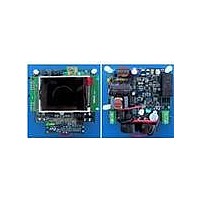
STEVAL-IHP001V3 STMicroelectronics, STEVAL-IHP001V3 Datasheet - Page 42

STEVAL-IHP001V3
Manufacturer Part Number
STEVAL-IHP001V3
Description
BOARD SMART PLUG STM32 SPZB260PR
Manufacturer
STMicroelectronics
Series
Zigbee™ SmartPlugr
Type
Microcontroller, Energy Meteringr
Specifications of STEVAL-IHP001V3
Frequency
2.4GHz
For Use With/related Products
STM32F10x, SPZB260-PRO, STPM01
Lead Free Status / RoHS Status
Lead free / RoHS Compliant
Other names
497-10677
Theory of operation
8.23
Figure 27. Timing for writing configuration and mode bits
42/60
The system that reads the data record from the STPM01 should check the integrity of each
data record. If the check fails, the reading should be repeated, but this time only the shifting
should be applied otherwise a new data would be latched into transmission latches and
incorrectly read one would be lost.
Normally, each byte is read out as most significant bit (MSB) first. But this can be changed
by setting the MSBF configuration bit in the STPM01 CFL data record. If this is done, each
byte is read out as least significant bit (LSB) first.
Writing procedure
Each writable bit (configuration and mode bits) has its own 6-bit absolute address. For the
configuration bits, the 6-bit address value corresponds to its decimal value, while for the
mode bits the addresses are the ones indicated in the Mode Signal paragraph.
In order to change the state of some latch one must send to STPM01 a byte of data which is
normal way to send data via SPI. This byte consists of 1-bit data to be latched (MSB),
followed by 6-bit address of destination latch, followed by 1-bit don’t care data (LSB) which
makes total 8 bits of command byte.
For example, if we would like to set the configuration bit 47 (part of the secondary current
channel calibrator) to 0, we must convert the decimal 47 to its 6-bit binary value: 101111.
The byte command will be then composed like this:
1 bit DATA value+6-bits address+1 bit (0 or 1) as depicted in
binary command will be 01011111 (0x5F) which is the one depicted in the figure or
01011110 (0x5E).
t
t
t
t
t
t
t
1
2
3
4
5
7
8
: Internal data transferred to SDATD
: SDATD data is stable and can be read
→ t
→ t
→ t
→ t
→ t
2
3
4
5
6
: Latching phase. Interval value > 2/f
: Data latched, SPI idle. Interval value > 30 ns
: Enable SPI for read operation. Interval value > 30 ns
: Serial clock counter is reset. Interval value > 30 ns
: SPI reset and enabled for read operation. Interval value > 30 ns
Doc ID 10853 Rev 7
CLK
Figure
27. In this case the
STPM01


