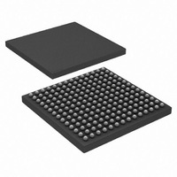
HSP50216KIZ Intersil, HSP50216KIZ Datasheet - Page 28

HSP50216KIZ
Manufacturer Part Number
HSP50216KIZ
Description
IC DOWNCONVERTER DGTL 4CH 196BGA
Manufacturer
Intersil
Datasheet
1.HSP50216KIZ.pdf
(58 pages)
Specifications of HSP50216KIZ
Function
Downconverter
Rf Type
W-CDMA
Package / Case
196-BGA
Lead Free Status / RoHS Status
Lead free / RoHS Compliant
Serial Data Output Time Slot Content/Format
Registers
These four registers are used to program the content and
format of the serial data output sequence time slots (see
Microprocessor Interface section:
Table 24, “SERIAL DATA OUTPUT 1 CONTENT/FORMAT
REGISTER 1 (IWA = *015h),” on page 39 through
Table 27, “SERIAL DATA OUTPUT 2 CONTENT/FORMAT
REGISTER 2 (IWA = *018h),” on page 40). There are seven
data time slots that make up a serial data output stream. The
number of data bits and data format of each slot is
programmable as well as whether there will be a sync
generated with the time slot (the syncs are only associated
with the SD1 serial outputs). Any of seven types of data or
zeros can be chosen for each time slot. Eight bits are used
to specify the content and format of each slot.
As an example, suppose we wanted to output 32-bit I and Q
values from channels 0 and 1 into the SD1A serial data
output stream, we would program the following settings in
the channel’s serial data output control and content/format
registers:
Channel 0:
delay = 0 (IWA = 0014h, bits 11:0 = 0);
first data time slot = I, 32-bit, sync pulse generated (IWA =
0015h, bits 7:0 = 0xC9);
second data time slot = Q, 32-bit, no sync pulse (IWA =
0015h, bits 15:8 = 0x4A);
third through seventh data time slot = zero and no sync, (IWA
= 0015h, bits 31:16 = 0 and IWA = 0016h, bits 31:0 = 0);
enable the SD1A serial output for this channel in the serial
routing mask (IWA = 0014h, bit 16 = 1).
28
HSP50216
Channel 1:
delay = 64 (IWA = 1014h, bits 11:0 = 0x40);
first data time slot = I, 32-bit, sync pulse generated (IWA =
1015h, bits 7:0 = 0xC9);
second data time slot = Q, 32-bit, no sync pulse (IWA =
1015h, bits 15:8 = 0x4A);
third through seventh data time slot = zero and no sync, (IWA
= 1015h, bits 31:16 = 0 and IWA = 1016h, bits 31:0 = 0);
enable the SD1A serial output for this channel in the serial
routing mask (IWA = 1014h, bit 16 = 1).
The resulting order is CH0 I first, then CH0 Q, CH1 I, and
CH1 Q with sync pulses generated in the I data slots. The
position of the sync pulses relative to the data slot may be
programmed with IWA register *014h bits 25:24.
Setting delay = 64 offsets channel 1’s 32 bit I and Q data by
64 clocks so that it immediately follows the 64 bits of data
from channel 0. In this way channel 1’s first and second time
slots follow channel 0’s second time slot.
Instead of using the delay to offset channel 1’s data, channel
0 could have been configured to output 32 bits of I in the fist
slot, 32 bits of Q in the second slot, 32 bits of zeros in the
third slot and 32 bits of zeros in the fourth slot. Channel 1
could then be configured to output 32 bits of zeros in the first
and second slots, 32 bits of I in the third slot and 32 bits of Q
in the fourth slot. As the channel outputs are OR’d together,
the zero slots do not interfere with data slots.
The HSP50216 Microprocessor (μP) interface consists of a
16-bit bidirectional data bus, P(15:0), three address pins,
ADD(2:0), a write strobe (WR), a read strobe (RD) and a
chip enable (CE). Indirect addressing is used for control and
configuration of the HSP50216. The control and
configuration data to be loaded is first written to a 32-bit
holding register at direct (external) addresses ADD(2:0) = 0
and 1, 16 bits at a time. The data is then transferred to the
target register, synchronous to the clock, by writing the
indirect (internal) address of the target register to direct
(external) address 2, ADD(2:0) = 2. The interface generates
a synchronous one clock cycle wide strobe to transfer the
data contained in the holding register to the target register.
The synchronization and write process requires 4 clock
periods. New data should not be written to the holding
register until after the synchronization period is over.
August 17, 2007
FN4557.6


