HSP50216KIZ Intersil, HSP50216KIZ Datasheet - Page 4
HSP50216KIZ
Manufacturer Part Number
HSP50216KIZ
Description
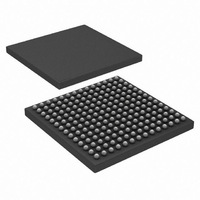
IC DOWNCONVERTER DGTL 4CH 196BGA
Manufacturer
Intersil
Datasheet
1.HSP50216KIZ.pdf
(58 pages)
Specifications of HSP50216KIZ
Function
Downconverter
Rf Type
W-CDMA
Package / Case
196-BGA
Lead Free Status / RoHS Status
Lead free / RoHS Compliant


Pin Descriptions
POWER SUPPLY
INPUTS
CONTROL
SYNCO
C(15:0)
RESET
A(15:0)
B(15:0)
SYNCI
NAME
ENIA
ENIB
ENIC
ENID
GND
VCC
D15
D14
D13
D12
D10
CLK
D11
D9
D8
D7
D6
D5
D4
D3
D2
D1
D0
TYPE
O
-
-
I
I
I
I
I
I
I
I
I
I
I
I
I
I
I
I
I
I
I
I
I
I
I
I
I
I
4
Positive Power Supply Voltage, 3.3V ±0.15
Ground, 0V.
Parallel Data Input bus A. Sampled on the rising edge of clock when ENIA is active (low).
Parallel Data Input bus B. Sampled on the rising edge of clock when ENIB is active (low).
Parallel Data Input bus C. Sampled on the rising edge of clock when ENIC is active (low).
Parallel Data Input D15 or tuner channel A COF.
Parallel Data Input D14 or tuner channel A COFSync.
Parallel Data Input D13 or tuner channel A SOF.
Parallel Data Input D12 or tuner channel A SOFSync.
Parallel Data Input D11 or tuner channel B COF.
Parallel Data Input D10 or tuner channel B COFSync.
Parallel Data Input D9 or tuner channel B SOF.
Parallel Data Input D8 or tuner channel B SOFSync.
Parallel Data Input D7 or tuner channel C COF.
Parallel Data Input D6 or tuner channel C COFSync.
Parallel Data Input D5 or tuner channel C SOF.
Parallel Data Input D4 or tuner channel C SOFSync.
Parallel Data Input D3 or tuner channel D COF.
Parallel Data Input D2 or tuner channel D COFSync.
Parallel Data Input D1 or tuner channel D SOF.
Parallel Data Input D0 or tuner channel D SOFSync.
Input enable for Parallel Data Input bus A. Active low. This pin enables the input to the part in one of two
modes, gated or interpolated. In gated mode, one sample is taken per CLK when ENI is asserted.
Input enable for Parallel Data Input bus B. Active low. This pin enables the input to the part in one of two
modes, gated or interpolated. In gated mode, one sample is taken per CLK when ENI is asserted.
Input enable for Parallel Data Input bus C. Active low. This pin enables the input to the part in one of two
modes, gated or interpolated. In gated mode, one sample is taken per CLK when ENI is asserted.
Input enable for Parallel Data Input bus D. Active low. This pin enables the input to the part in one of two
modes, gated or interpolated. In gated mode, one sample is taken per CLK when ENI is asserted.
Input clock. All processing in the HSP50216 occurs on the rising edge of CLK.
Synchronization Input Signal. Used to align the processing with an external event or with other HSP50216
devices. SYNCI can update the carrier NCO, reset decimation counters, restart the filter compute engine,
and restart the output section among other functions. For most of the functional blocks, the response to
SYNCI is programmable and can be enabled or disabled.
Synchronization Output Signal. The processing of multiple HSP50216 devices can be synchronized by
tying the SYNCO from one HSP50216 device (the master) to the SYNCI of all the HSP50216 devices (the
master and slaves).
Reset Signal. Active low. Asserting reset will halt all processing and set certain registers to default values.
HSP50216
DESCRIPTION
August 17, 2007
FN4557.6
Related parts for HSP50216KIZ
Image
Part Number
Description
Manufacturer
Datasheet
Request
R

Part Number:
Description:
Intersil Corporation [CMOS Serial Controller Interface]
Manufacturer:
Intersil Corporation
Datasheet:
Part Number:
Description:
Manufacturer:
Intersil Corporation
Datasheet:
Part Number:
Description:
357-036-542-201 CARDEDGE 36POS DL .156 BLK LOPRO
Manufacturer:
Intersil Corporation
Datasheet:
Part Number:
Description:
1024-Word x 4-Bit LSI Static RAM
Manufacturer:
Intersil Corporation
Datasheet:
Part Number:
Description:
General Purpose NPN Transistor Arrays FN341.4
Manufacturer:
Intersil Corporation
Datasheet:
Part Number:
Description:
CMOS 16-Bit Microprocessor
Manufacturer:
Intersil Corporation
Datasheet:
Part Number:
Description:
Manufacturer:
Intersil Corporation
Datasheet:
Part Number:
Description:
Manufacturer:
Intersil Corporation
Datasheet:
Part Number:
Description:
Manufacturer:
Intersil Corporation
Datasheet:
Part Number:
Description:
Manufacturer:
Intersil Corporation
Datasheet:
Part Number:
Description:
CMOS 6-Bit Latch and Decoder Memory Interfaces
Manufacturer:
Intersil Corporation
Datasheet:
Part Number:
Description:
CA3046General Purpose NPN Transistor Arrays
Manufacturer:
Intersil Corporation
Datasheet:
Part Number:
Description:
Manufacturer:
Intersil Corporation
Datasheet:
Part Number:
Description:
TR909 DLC/FLC SLIC with Low Power Standby
Manufacturer:
Intersil Corporation
Datasheet:
Part Number:
Description:
Manufacturer:
Intersil Corporation
Datasheet: