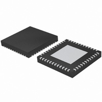
TDA9899HN/V2,551 NXP Semiconductors, TDA9899HN/V2,551 Datasheet - Page 43

TDA9899HN/V2,551
Manufacturer Part Number
TDA9899HN/V2,551
Description
IC IF PROCESSOR MULTISTD 48HVQFN
Manufacturer
NXP Semiconductors
Datasheet
1.TDA9899HLV2151.pdf
(103 pages)
Specifications of TDA9899HN/V2,551
Function
IF Processor
Rf Type
ATV, DVB, FM
Package / Case
48-VFQFN Exposed Pad
Lead Free Status / RoHS Status
Lead free / RoHS Compliant
Other names
935282856551
TDA9899HN/V2-S
TDA9899HN/V2-S
TDA9899HN/V2-S
TDA9899HN/V2-S
- Current page: 43 of 103
- Download datasheet (498Kb)
NXP Semiconductors
Table 55.
V
f
for L); IF input from 50
B/G is 10 % and for L is 3 %; video signal in accordance with “ITU-T J.63 line 17 and line 330” or “NTC-7 Composite”;
internal Nyquist slope switched on (W7[0] = 0); not dual mode; measurements taken in test circuit of
otherwise specified.
TDA9899_3
Product data sheet
Symbol
I
V
VIF AGC; pin CIFAGC
I
I
I
VIF AGC control; pin AGCVIN
I
I
V
V
Tuner AGC; pin TAGC
Integral TAGC loop mode (W6[7:6] = 10); TAGC is current output; applicable for negative modulation only; unmodulated VIF;
see
V
I
I
R
V
SC
sink(o)
ch(max)
ch(add)
dch
sink(i)(max)
source(i)(max)
source
sink
P
G
acc(set)TOP
OH
i(max)
AGCVIN
i(IF)(RMS)
sat(u)
L
= 5 V; T
acc(set)TOP
= 32.875 MHz; PC / SC = 13 dB; f
VIF
Table 48
/ V
AGCVIN
amb
Characteristics
/ T
and
= 25 C; see
Figure 12
Parameter
output sink current
HIGH-level output voltage
maximum charge current
additional charge current
discharge current
maximum input sink current
maximum input source
current
maximum input voltage
voltage on pin AGCVIN
change of VIF gain with
voltage on pin AGCVIN
RMS IF input voltage
TOP setting accuracy
source current
sink current
TOP setting accuracy
variation with temperature
load resistance
upper saturation voltage
via broadband transformer 1 : 1; video modulation: Vestigial SideBand (VSB); residual carrier for
Table 26
…continued
for input frequencies; B/G standard is used for the specification (f
AF
= 400 Hz); input level V
Rev. 03 — 15 January 2008
Conditions
W7[3] = 0
W7[3] = 1
L standard
L standard: in the event of
missing VITS pulses and
no white video content
L standard; normal mode
L standard; fast mode
V
at starting point of tuner
AGC takeover;
I
TAGC charge current
TAGC discharge current;
V
W9[4:0] = 1 0000
pin operating as current
output
sink(TAGC)
AGCVIN
TAGC
W9[4:0] = 0 0000
W9[4:0] = 1 0000
W9[4:0] = 1 1111
normal mode
fast mode activated by
internal level detector
= 1 V
Multistandard hybrid IF processing including car mobile
= 2.8 V
= 100 A
i(IF)
= 10 mV (RMS) (sync level for B/G; peak white level
[3]
[3]
[3]
[3]
[3]
Min
-
-
-
75
-
-
-
-
-
-
1
-
-
-
-
0.20
7
400
-
50
V
2
P
0.3 -
Typ
-
-
-
100
100
35
1.8
-
-
-
-
57.9
78.7
98.2
-
0.27
10
500
-
-
75
Figure
PC
TDA9899
© NXP B.V. 2008. All rights reserved.
= 38.375 MHz;
Max
3
10
V
125
-
-
-
1
1
V
3.5
-
-
-
-
+2
0.34
13
600
0.02
-
-
P
P
49; unless
+ 0.5 V
Unit
mA
nA
nA
V
V
dB/V
dB V
dB V
dB V
dB
dB/K
M
V
43 of 103
A
A
A
A
A
A
A
A
Related parts for TDA9899HN/V2,551
Image
Part Number
Description
Manufacturer
Datasheet
Request
R

Part Number:
Description:
IC IF PROCESSOR MULTISTD 48HVQFN
Manufacturer:
NXP Semiconductors
Datasheet:
Part Number:
Description:
Up-Down Converters MULTI APPL SYS FOR TERRESTR IF
Manufacturer:
NXP Semiconductors
Part Number:
Description:
Up-Down Converters MULTI APPL SYS FOR TERRESTR IF
Manufacturer:
NXP Semiconductors
Part Number:
Description:
Tda9899 Multistandard Hybrid If Processing Including Car Mobile
Manufacturer:
NXP Semiconductors
Datasheet:
Part Number:
Description:
NXP Semiconductors designed the LPC2420/2460 microcontroller around a 16-bit/32-bitARM7TDMI-S CPU core with real-time debug interfaces that include both JTAG andembedded trace
Manufacturer:
NXP Semiconductors
Datasheet:

Part Number:
Description:
NXP Semiconductors designed the LPC2458 microcontroller around a 16-bit/32-bitARM7TDMI-S CPU core with real-time debug interfaces that include both JTAG andembedded trace
Manufacturer:
NXP Semiconductors
Datasheet:
Part Number:
Description:
NXP Semiconductors designed the LPC2468 microcontroller around a 16-bit/32-bitARM7TDMI-S CPU core with real-time debug interfaces that include both JTAG andembedded trace
Manufacturer:
NXP Semiconductors
Datasheet:
Part Number:
Description:
NXP Semiconductors designed the LPC2470 microcontroller, powered by theARM7TDMI-S core, to be a highly integrated microcontroller for a wide range ofapplications that require advanced communications and high quality graphic displays
Manufacturer:
NXP Semiconductors
Datasheet:
Part Number:
Description:
NXP Semiconductors designed the LPC2478 microcontroller, powered by theARM7TDMI-S core, to be a highly integrated microcontroller for a wide range ofapplications that require advanced communications and high quality graphic displays
Manufacturer:
NXP Semiconductors
Datasheet:
Part Number:
Description:
The Philips Semiconductors XA (eXtended Architecture) family of 16-bit single-chip microcontrollers is powerful enough to easily handle the requirements of high performance embedded applications, yet inexpensive enough to compete in the market for hi
Manufacturer:
NXP Semiconductors
Datasheet:
Part Number:
Description:
The XA-S3 device is a member of Philips Semiconductors? XA(eXtended Architecture) family of high performance 16-bitsingle-chip microcontrollers
Manufacturer:
NXP Semiconductors
Datasheet:

Part Number:
Description:
The NXP BlueStreak LH75401/LH75411 family consists of two low-cost 16/32-bit System-on-Chip (SoC) devices
Manufacturer:
NXP Semiconductors
Datasheet:

Part Number:
Description:
The NXP LPC3130/3131 combine an 180 MHz ARM926EJ-S CPU core, high-speed USB2
Manufacturer:
NXP Semiconductors
Datasheet:

Part Number:
Description:
The NXP LPC3141 combine a 270 MHz ARM926EJ-S CPU core, High-speed USB 2
Manufacturer:
NXP Semiconductors


