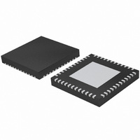
TDA9899HN/V2,551 NXP Semiconductors, TDA9899HN/V2,551 Datasheet - Page 6

TDA9899HN/V2,551
Manufacturer Part Number
TDA9899HN/V2,551
Description
IC IF PROCESSOR MULTISTD 48HVQFN
Manufacturer
NXP Semiconductors
Datasheet
1.TDA9899HLV2151.pdf
(103 pages)
Specifications of TDA9899HN/V2,551
Function
IF Processor
Rf Type
ATV, DVB, FM
Package / Case
48-VFQFN Exposed Pad
Lead Free Status / RoHS Status
Lead free / RoHS Compliant
Other names
935282856551
TDA9899HN/V2-S
TDA9899HN/V2-S
TDA9899HN/V2-S
TDA9899HN/V2-S
- Current page: 6 of 103
- Download datasheet (498Kb)
NXP Semiconductors
Table 1.
V
[1]
[2]
[3]
TDA9899_3
Product data sheet
Symbol
G
G
f
C/N
Digital zero IF
V
G
G
f
Reference frequency input from external source
f
V
synth
synth
ref
P
n(synth)
ripple(pb)LIF
stpb
image
n(synth)
o(dif)(p-p)
ref(RMS)
IF(max)
IF(cr)
IF(max)
IF(cr)
= 5 V; T
Values of video and sound parameters can be decreased at V
AC load; C
carrier traps.
The sound carrier trap can be bypassed by setting the I
spectrum appears at pin CVBS. The video amplitude is reduced to 1.1 V (p-p).
amb
Quick reference data
L
Parameter
maximum IF gain
control range IF gain
synthesizer frequency
synthesizer phase noise
low IF pass-band ripple
stop-band attenuation
image rejection
carrier-to-noise ratio
peak-to-peak differential output
voltage
maximum IF gain
control range IF gain
synthesizer frequency
synthesizer phase noise
reference frequency
RMS reference voltage
= 25 C.
< 20 pF and R
L
> 1 k . The sound carrier frequencies (depending on TV standard) are attenuated by the integrated sound
…continued
Rev. 03 — 15 January 2008
Conditions
output peak-to-peak level to
input RMS level ratio
see
with 4 MHz crystal oscillator
reference; f
f
6 MHz bandwidth
7 MHz bandwidth
8 MHz bandwidth
8 MHz band; f = 15.75 MHz
at f
V
see
between pin OUT1A and
pin OUT1B or between
pin OUT2A and pin OUT2B;
W4[7] = 0
output peak-to-peak level to
input RMS level ratio
see
with 4 MHz crystal oscillator
reference; f
f
W7[7] = 0
W7[7] = 0; see
and
IF
IF
10 MHz to 0 MHz; BP on
i(IF)
at 1 kHz
at 10 kHz
at 100 kHz
at 1.4 MHz
at 1 kHz
at 10 kHz
at 100 kHz
at 1.4 MHz
2
= 36 MHz
= 36 MHz
o
C-bus bit W2[0] to logic 0; see
Table 37
Figure 38
Table 37
Figure 47
= 4.9 MHz;
= 10 mV (RMS);
Multistandard hybrid IF processing including car mobile
P
= 4.5 V.
synth
synth
and
and
Figure 35
= 31 MHz;
= 31 MHz;
Table 38
Table 38
[8][9][10]
Table
[11]
[8]
[8]
[8]
[8]
[8]
[8]
[7]
[8]
[8]
[8]
[8]
[8]
[8]
25. In this way the full composite video
Min
-
60
-
89
89
98
115
-
-
-
30
30
112
-
-
60
-
89
89
98
115
-
15
Typ
89
66
-
99
99
102
119
-
-
-
40
34
118
2
89
66
-
99
99
102
119
4
150
TDA9899
© NXP B.V. 2008. All rights reserved.
Max
-
-
-
-
-
-
-
2.7
2.7
2.7
-
-
-
-
-
-
-
-
-
-
-
-
500
Unit
dB
dB
MHz
dBc/Hz
dBc/Hz
dBc/Hz
dBc/Hz
dB
dB
dB
dB
dB
dBc/Hz
V
dB
dB
MHz
dBc/Hz
dBc/Hz
dBc/Hz
dBc/Hz
MHz
mV
6 of 103
Related parts for TDA9899HN/V2,551
Image
Part Number
Description
Manufacturer
Datasheet
Request
R

Part Number:
Description:
IC IF PROCESSOR MULTISTD 48HVQFN
Manufacturer:
NXP Semiconductors
Datasheet:
Part Number:
Description:
Up-Down Converters MULTI APPL SYS FOR TERRESTR IF
Manufacturer:
NXP Semiconductors
Part Number:
Description:
Up-Down Converters MULTI APPL SYS FOR TERRESTR IF
Manufacturer:
NXP Semiconductors
Part Number:
Description:
Tda9899 Multistandard Hybrid If Processing Including Car Mobile
Manufacturer:
NXP Semiconductors
Datasheet:
Part Number:
Description:
NXP Semiconductors designed the LPC2420/2460 microcontroller around a 16-bit/32-bitARM7TDMI-S CPU core with real-time debug interfaces that include both JTAG andembedded trace
Manufacturer:
NXP Semiconductors
Datasheet:

Part Number:
Description:
NXP Semiconductors designed the LPC2458 microcontroller around a 16-bit/32-bitARM7TDMI-S CPU core with real-time debug interfaces that include both JTAG andembedded trace
Manufacturer:
NXP Semiconductors
Datasheet:
Part Number:
Description:
NXP Semiconductors designed the LPC2468 microcontroller around a 16-bit/32-bitARM7TDMI-S CPU core with real-time debug interfaces that include both JTAG andembedded trace
Manufacturer:
NXP Semiconductors
Datasheet:
Part Number:
Description:
NXP Semiconductors designed the LPC2470 microcontroller, powered by theARM7TDMI-S core, to be a highly integrated microcontroller for a wide range ofapplications that require advanced communications and high quality graphic displays
Manufacturer:
NXP Semiconductors
Datasheet:
Part Number:
Description:
NXP Semiconductors designed the LPC2478 microcontroller, powered by theARM7TDMI-S core, to be a highly integrated microcontroller for a wide range ofapplications that require advanced communications and high quality graphic displays
Manufacturer:
NXP Semiconductors
Datasheet:
Part Number:
Description:
The Philips Semiconductors XA (eXtended Architecture) family of 16-bit single-chip microcontrollers is powerful enough to easily handle the requirements of high performance embedded applications, yet inexpensive enough to compete in the market for hi
Manufacturer:
NXP Semiconductors
Datasheet:
Part Number:
Description:
The XA-S3 device is a member of Philips Semiconductors? XA(eXtended Architecture) family of high performance 16-bitsingle-chip microcontrollers
Manufacturer:
NXP Semiconductors
Datasheet:

Part Number:
Description:
The NXP BlueStreak LH75401/LH75411 family consists of two low-cost 16/32-bit System-on-Chip (SoC) devices
Manufacturer:
NXP Semiconductors
Datasheet:

Part Number:
Description:
The NXP LPC3130/3131 combine an 180 MHz ARM926EJ-S CPU core, high-speed USB2
Manufacturer:
NXP Semiconductors
Datasheet:

Part Number:
Description:
The NXP LPC3141 combine a 270 MHz ARM926EJ-S CPU core, High-speed USB 2
Manufacturer:
NXP Semiconductors


